Press release
CyberOptics Semiconductor to Discuss Wafer Sensor Position Systems During ISMI Manufacturing Week
Mark Hannaford, Director of Sales and Marketing at CyberOptics Semiconductor (www.cyberopticssemi.com) will conduct a presentation on the company’s WaferSense family of products including its wireless set of measurement solutions for leveling, gapping and teaching semiconductor equipment during ISMI Manufacturing Week in Austin, TX next week. Specifically, Mark will discuss how CyberOptics Auto Teach System, Auto Gapping Systems and other WaferSense technology has helped users improve costs, productivity, reliability, manufacturing as well as purity during the ISMI Second Source Supplier Workshop to be held on Monday, November 1, 2010.CyberOptics’ WaferSense family of products offers a wireless set of measurement solutions for leveling, gapping and teaching semiconductor equipment. Each product boasts a wafer-like form factor allowing them to travel like wafers travel, making for easy installation and minimal machine downtime. Because they are wireless, WaferSense products save time and are easy to use. The wireless feature also allows you to obtain data from locations that are difficult to access otherwise.
For more information on CyberOptics family of WaferSense technology including its Auto Teaching System, Auto Gapping System and Auto Vibration System, refer to the website at http://www.cyberopticssemi.com/products/wafersense/ or contact sales at (503) 495-2200 for more information.
About CyberOptics Semiconductor, Inc.
CyberOptics Semiconductor develops automated products that seamlessly measure critical parameters in semiconductor fabrication processes and equipment. The company’s pioneering WaferSense® line includes wireless metrology devices for vibration, leveling, gapping, teaching and sensing airborne particles in semiconductor process equipment. The company is the largest producer of reflective wafermapping sensors and a leading provider of frame grabber machine vision boards under its HAMA Sensors™ and Imagenation™ brands. CyberOptics Semiconductor is a subsidiary of CyberOptics Corp. (Nasdaq:CYBE), one of the world's leading providers of process yield and throughput improvement solutions for the electronic assembly and semiconductor fabrication industries. For information, visit http://www.cyberopticssemi.com/, e-mail CSsales@cyberoptics.com or call 800-366-9131.
9130 SW Pioneer Court, Suite D Wilsonville, OR 97070 USA
This release was published on openPR.
Permanent link to this press release:
Copy
Please set a link in the press area of your homepage to this press release on openPR. openPR disclaims liability for any content contained in this release.
You can edit or delete your press release CyberOptics Semiconductor to Discuss Wafer Sensor Position Systems During ISMI Manufacturing Week here
News-ID: 149943 • Views: …
More Releases from CyberOptics Semiconductor
CyberOptics Semiconductor to Demo Final Production Version of WaferSense® Airbo …
CyberOptics Semiconductors (www.cyberopticssemi.com) will demonstrate the final production version of the WaferSense® Airborne Particle Sensor (APS) during Semicon Japan in booth number 5B-204. The company will also feature its full line of WaferSense wireless metrology devices at the international trade show scheduled for December 5 – 7, 2011 at the Makuhari Messe in Chiba, Japan.
Addressing the limitations of traditional airborne particle with limited reach and static output, the WaferSense…
450 mm Wireless Wafer Processing Metrology Sensors Support Next-Generation of Se …
CyberOptics Semiconductor offers a line of wireless 450 mm wafer processing metrology sensors to help chipmakers and tool manufacturers qualify next-generation semiconductor production processes.
CyberOptics’ 450 mm carbon fiber WaferSense® sensors are designed to obtain precise metrology data to optimize new processing equipment for shrinking 32 nm and 22 nm process tolerances, according to Craig C. Ramsey, Ph.D., CyberOptics Semiconductor’s general manager.
CyberOptics’ 450 mm sensors allow engineers to level…
CyberOptics Semiconductor to Discuss Solutions for Semiconductor Tool Qualificat …
CyberOptics Semiconductor (cyberopticssemi.com) will discuss how a “Wireless Particle Counting Wafer Improves Semiconductor Tool Qualification” during ISMI Manufacturing Week 2011 to be held in Austin, TX during October 17 - 21. During ISMI Manufacturing Week, Allyn Jackson, CyberOptics Technical Support Manager, will explain how the WaferSense® Airborne Particle Sensor offers faster, more accurate qualification of process tools than traditional particle measurement methods such as monitor wafers and bench-top counters.…
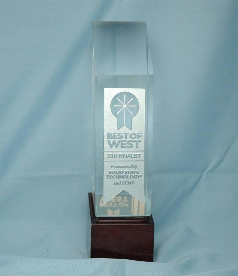
CyberOptics Airborne Particle Sensor Honored at Semicon West
The WaferSense® Airborne Particle Sensor from CyberOptics Semiconductor was chosen as a finalist in The Best of the West 2011 Awards sponsored by Solid State Technology and SEMI at Semicon West in recognizing important product and technology developments in the microelectronics industries. Best of West finalists and award recipients were selected based on the submission’s financial impact on the industry, engineering or scientific achievement, or societal impact and benefits,…
More Releases for WaferSense
CyberOptics Semiconductor to Demo Final Production Version of WaferSense® Airbo …
CyberOptics Semiconductors (www.cyberopticssemi.com) will demonstrate the final production version of the WaferSense® Airborne Particle Sensor (APS) during Semicon Japan in booth number 5B-204. The company will also feature its full line of WaferSense wireless metrology devices at the international trade show scheduled for December 5 – 7, 2011 at the Makuhari Messe in Chiba, Japan.
Addressing the limitations of traditional airborne particle with limited reach and static output, the WaferSense…
CyberOptics Airborne Particle Sensor Honored at Semicon West
The WaferSense® Airborne Particle Sensor from CyberOptics Semiconductor was chosen as a finalist in The Best of the West 2011 Awards sponsored by Solid State Technology and SEMI at Semicon West in recognizing important product and technology developments in the microelectronics industries. Best of West finalists and award recipients were selected based on the submission’s financial impact on the industry, engineering or scientific achievement, or societal impact and benefits,…
Vibration Sensor Helps Diffusion Furnace Team Identify Vibration Sources to Incr …
When a diffusion furnace team at a 200 mm fab experienced defect problems in specific stocker locations of its high volume semiconductor process, CyberOptics WaferSense® Auto Vibration Sensors helped test a theory that excessive vibrations created by stocker fans effected die yield.
Shaped like a wafer, WaferSense Auto Vibration Sensors (AVS) can travel along an entire wafer path, collecting, recording and displaying exact vibration exposure. Placed either in standard…
CyberOptics Semiconductor To Demo WaferSense® Airborne Particle Sensor at Semic …
CyberOptics Semiconductor will demo its new WaferSense® Airborne Particle Sensor (cyberopticssemi.com/products/wafersense/aps) along other WaferSense wireless metrology devices including the Auto Leveling System and Auto Vibration System, during Semicon West 2011 in Booth No. 2406. CyberOptics’ WaferSense family of products offers a wireless set of measurement solutions for leveling, gapping and teaching semiconductor equipment.
Introduced in January 2011 after a year of beta testing and research, the WaferSense Airborne Particle Sensor…
CyberOptics WaferSense® Auto Gapping System Helps 300mm Wafer Fab Increase Tool …
CyberOptics Semiconductors (www.CyberOpticsSemi.com) has published an application note on its web site explaining how its WaferSense® Auto Gapping System (AGS) has helped a 300 mm fab increase the availability of a plasma‐enhanced chemical vapor deposition (PECVD) tool.
The Auto Gapping System replaced a legacy gapping method that took 10 hours to measure the distance between the chamber’s gas showerhead and wafer pedestal to ensure uniform film deposition, particularly…
CyberOptics WaferSense® Sensors Helps 200mm Wafer Fab Trace Reduced Yield to Vi …
CyberOptics Semiconductors has published an application note on its web site discussing how its WaferSense® Vibration and Leveling Sensors helped a vertical diffusion group characterize various causes of wafer damage that occurred during high‐volume processing of wafers in a boat.
Wafer breakage, micro scratching and particle contamination were reducing yield in a fab’s 200 mm high volume process. Misaligned wafers in crowded cassettes and tool vibration created by environmental…
