Press release
CyberOptics WaferSense® Sensors Helps 200mm Wafer Fab Trace Reduced Yield to Vibration Sources and Wafer Leveling
CyberOptics Semiconductors has published an application note on its web site discussing how its WaferSense® Vibration and Leveling Sensors helped a vertical diffusion group characterize various causes of wafer damage that occurred during high‐volume processing of wafers in a boat.Wafer breakage, micro scratching and particle contamination were reducing yield in a fab’s 200 mm high volume process. Misaligned wafers in crowded cassettes and tool vibration created by environmental forces, including fans, failing robotic components and carts moving along the aisle’s perforated floor were suspected causes of reduced yield. Wafers were vulnerable to damage during high volume handling at the load port, in the cassettes with narrow pitch and as they ascended a long Z axis and were exposed to the hot furnace.
Placing a WaferSense Vibration Sensor and Leveling Sensor in the same cassette, the fabricator conducted a series of tests, comparing the same tool movements at different locations in the process to characterize wafer damage causes.
A wireless and wafer like inclinometer, the WaferSense Auto Leveling Sensor captures the inclination of previously out-of-reach semiconductor process equipment. Unlike traditional methods, the Auto Leveling Sensor doesn't require equipment disassembly or disruptions to vacuum chambers, reducing calibration time by 80% or more. The WaferSense Auto Vibration Sensor moves through semiconductor process equipment to monitor three-axis accelerations and vibrations. A wafer-like shape is compatible with existing automation and wireless communications provide real-time data to speed tool setup and maintenance.
For the 200mm fab analysis, the vacuum‐compatible sensors measured wafer vibration in x, y and z dimensions and wafer tilt in x, y dimensions while cassettes moved throughout wafer‐handling stations in the diffusion process: from the load port to the CZ stage, from storage rack to transfer rack and into the cooled furnace. Wafer tilt and vibration also were measured in a storage rack with the fan on and off and as engineers ran carts at various speeds and weights in the aisle next to storage and transfer racks.
The real‐time data from the wireless sensors on tool vibration and leveling allowed engineers to make immediate adjustments and re‐characterize the diffusion process. Co‐planarity established among wafer‐handling stations ensures proper wafer tilt in cassettes and prevents wafer damage throughout the process.
For specific details on how CyberOptics’ WaferSense Auto Leveling and Auto Vibration Sensors worked in unison to solve yield problems for the 200 mm fab, please go to our web site at: http://www.cyberopticssemi.com/content/files/news/documents/reports_from_the_fab0810.pdf
Detailed information on CyberOptics’ WaferSense products is available online at http://www.cyberopticssemi.com/products or by contacting sales at (503) 495-2200 for more information.
CyberOptics Semiconductor develops automated products that seamlessly measure critical parameters in semiconductor fabrication processes and equipment. The company’s pioneering WaferSense® line includes wireless metrology devices for vibration, leveling, gapping, teaching and sensing airborne particles in semiconductor process equipment. The company is the largest producer of reflective wafermapping sensors and a leading provider of frame grabber machine vision boards under its HAMA Sensors™ and Imagenation™ brands. CyberOptics Semiconductor is a subsidiary of CyberOptics Corp. (Nasdaq:CYBE), one of the world's leading providers of process yield and throughput improvement solutions for the electronic assembly and semiconductor fabrication industries. For information, visit http://www.cyberopticssemi.com/, e-mail CSsales@cyberoptics.com or call 800-366-9131.
9130 SW Pioneer Court, Suite D Wilsonville, OR 97070
This release was published on openPR.
Permanent link to this press release:
Copy
Please set a link in the press area of your homepage to this press release on openPR. openPR disclaims liability for any content contained in this release.
You can edit or delete your press release CyberOptics WaferSense® Sensors Helps 200mm Wafer Fab Trace Reduced Yield to Vibration Sources and Wafer Leveling here
News-ID: 164103 • Views: …
More Releases from CyberOptics Semiconductor
CyberOptics Semiconductor to Demo Final Production Version of WaferSense® Airbo …
CyberOptics Semiconductors (www.cyberopticssemi.com) will demonstrate the final production version of the WaferSense® Airborne Particle Sensor (APS) during Semicon Japan in booth number 5B-204. The company will also feature its full line of WaferSense wireless metrology devices at the international trade show scheduled for December 5 – 7, 2011 at the Makuhari Messe in Chiba, Japan.
Addressing the limitations of traditional airborne particle with limited reach and static output, the WaferSense…
450 mm Wireless Wafer Processing Metrology Sensors Support Next-Generation of Se …
CyberOptics Semiconductor offers a line of wireless 450 mm wafer processing metrology sensors to help chipmakers and tool manufacturers qualify next-generation semiconductor production processes.
CyberOptics’ 450 mm carbon fiber WaferSense® sensors are designed to obtain precise metrology data to optimize new processing equipment for shrinking 32 nm and 22 nm process tolerances, according to Craig C. Ramsey, Ph.D., CyberOptics Semiconductor’s general manager.
CyberOptics’ 450 mm sensors allow engineers to level…
CyberOptics Semiconductor to Discuss Solutions for Semiconductor Tool Qualificat …
CyberOptics Semiconductor (cyberopticssemi.com) will discuss how a “Wireless Particle Counting Wafer Improves Semiconductor Tool Qualification” during ISMI Manufacturing Week 2011 to be held in Austin, TX during October 17 - 21. During ISMI Manufacturing Week, Allyn Jackson, CyberOptics Technical Support Manager, will explain how the WaferSense® Airborne Particle Sensor offers faster, more accurate qualification of process tools than traditional particle measurement methods such as monitor wafers and bench-top counters.…
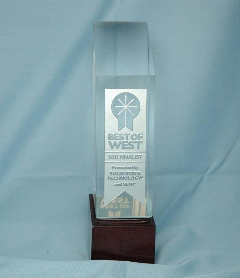
CyberOptics Airborne Particle Sensor Honored at Semicon West
The WaferSense® Airborne Particle Sensor from CyberOptics Semiconductor was chosen as a finalist in The Best of the West 2011 Awards sponsored by Solid State Technology and SEMI at Semicon West in recognizing important product and technology developments in the microelectronics industries. Best of West finalists and award recipients were selected based on the submission’s financial impact on the industry, engineering or scientific achievement, or societal impact and benefits,…
More Releases for Wafer
Wafer Surface Thinning Machine Market 2026-2032: Fully Automatic Wafer Grinders, …
Global Leading Market Research Publisher QYResearch announces the release of its latest report "Wafer Surface Thinning Machine - Global Market Share and Ranking, Overall Sales and Demand Forecast 2026-2032". For semiconductor fabs, OSATs (outsourced semiconductor assembly and test providers), and institutional investors tracking advanced packaging, the wafer back-grinding process has emerged as a critical bottleneck and differentiator. As 3D stacking, fan-out wafer-level packaging (FOWLP), and power device miniaturization intensify, the…
Semiconductor Silicon Wafer Market Is Going to Boom |• Silicon Wafer • Globa …
Worldwide Market Reports has released a new in-depth research study on the "Semiconductor Silicon Wafer Market," highlighting strong growth potential in the coming years. The report delivers a structured and data-driven analysis of the market landscape, combining robust research methodology, market sizing, validated data modeling, and insights sourced from reliable primary and secondary channels.
The study thoroughly examines key market aspects, including growth drivers, restraints, challenges, emerging opportunities, technological advancements, innovation…
Wafer Hybrid Bonding Equipment Market Share Driven by Wafer-to-Wafer Technology …
Wafer Hybrid Bonding Equipment Market Size
The global market for Wafer Hybrid Bonding Equipment was valued at US$ 164 million in the year 2024 and is projected to reach a revised size of US$ 756 million by 2031, growing at a CAGR of 24.7% during the forecast period.
View sample report
https://reports.valuates.com/request/sample/QYRE-Auto-31W14822/Global_Wafer_Hybrid_Bonding_Equipment_Market_Insights_Forecast_to_2029
The Wafer Hybrid Bonding Equipment market is experiencing accelerated growth, driven by increasing demand for advanced semiconductor packaging technologies that enable higher…
Semiconductor Wafer Electrostatic Chucks for 300mm Wafer Market
Semiconductor Wafer Electrostatic Chucks for 300mm Wafer Market
The global Semiconductor Wafer Electrostatic Chucks for 300mm Wafer market was valued at US$ 1165 million in 2023 and is anticipated to reach US$ 1672.7 million by 2030, witnessing a CAGR of 5.3% during the forecast period 2024-2030.
View Sample Report
https://reports.valuates.com/request/sample/QYRE-Auto-38F13137/Global_Semiconductor_Wafer_Electrostatic_Chucks_for_300mm_Wafer_Market_Research_Report_2023
Report Scope
The Semiconductor Wafer Electrostatic Chucks for 300mm Wafer market size, estimations, and forecasts are provided in terms of output/shipments (Units) and revenue…
Automatic Mounter Wafer Equipment Market Report 2018: Segmentation by Type (100 …
Global Automatic Mounter Wafer Equipment market research report provides company profile for Lintec Corporation, Nitto Denko, Tokyo Electron, Technovision, Takatori, Ultron Systems, DISCO Corp., Syagrus Systems, Advanced Dicing Technologies, Longhill Industries and Others.
This market study includes data about consumer perspective, comprehensive analysis, statistics, market share, company performances (Stocks), historical analysis 2012 to 2017, market forecast 2018 to 2025 in terms of volume, revenue, YOY growth rate, and CAGR for…
EMEA Solar Wafer Cutting Fluid PEG Market For Semiconductor, Solar Wafer, Crysta …
Latest industry research report on: EMEA (Europe, Middle East and Africa) Solar Wafer Cutting Fluid PEG Market : Industry Size, Share, Research, Reviews, Analysis, Strategies, Demand, Growth, Segmentation, Parameters, Forecasts
Request For Sample Report @ https://www.marketresearchreports.biz/sample/sample/1194694
Geographically, this report split EMEA into Europe, the Middle East and Africa, With sales (K MT), revenue (Million USD), market share and growth rate of Solar Wafer Cutting Fluid PEG for these regions, from 2012 to…
