


Press release
Global mSAP Substrate Market Outlook: High-Density Interconnect, Semiconductor Packaging, and AI Infrastructure Growth

Global Leading Market Research Publisher QYResearch announces the release of its latest report "mSAP Substrate for AI - Global Market Share and Ranking, Overall Sales and Demand Forecast 2026-2032". Based on current situation and impact historical analysis (2021-2025) and forecast calculations (2026-2032), this report provides a comprehensive analysis of the global mSAP Substrate for AI market, including market size, share, demand, industry development status, and forecasts for the next few years.
The exponential growth of artificial intelligence workloads, from large language model training to edge inference, has placed unprecedented demands on semiconductor packaging technologies. Traditional substrate solutions are struggling to meet the bandwidth, signal integrity, and thermal dissipation requirements of today's most advanced AI accelerators. Modified semi-additive process (mSAP) substrates have emerged as a critical enabler for high-performance computing (HPC) and advanced packaging architectures, delivering micron-level line widths and spacing that support the high I/O densities demanded by modern AI processors. These specialized substrates address the core industry pain point of scaling interconnect density while maintaining signal integrity and heat dissipation-a challenge that has become the bottleneck in next-generation AI system performance. According to QYResearch's latest industry analysis, the global market for mSAP Substrate for AI was estimated to be worth US$ 1,748 million in 2025 and is projected to reach US$ 3,549 million, growing at a CAGR of 10.8% from 2026 to 2032, reflecting the accelerating adoption of AI-optimized packaging solutions.
【Get a free sample PDF of this report (Including Full TOC, List of Tables & Figures, Chart)】
https://www.qyresearch.com/reports/6116555/msap-substrate-for-ai
Manufacturing Process and Supply Chain Architecture
mSAP substrates represent a significant technological advancement over traditional subtractive etching processes. The modified semi-additive process achieves micron-level line widths and spacing-down to 3/3 μm and below-on an extremely thin seed layer, enabling the high-density interconnects essential for AI accelerator packaging. Shipments of these products reached approximately 380,000 square meters in 2024, with an average unit price estimated at approximately US$4,600 per square meter. Typical annual production capacity per manufacturing line is estimated at approximately 60,000 square meters, underscoring the capital-intensive nature of this specialized fabrication segment.
The industry supply chain comprises distinct upstream, midstream, and downstream segments. Upstream suppliers provide critical materials including polymer substrates and ABF (Ajinomoto Build-up Film) films, ultra-thin copper foil, electroless plating solutions, photolithography and development materials, and precision manufacturing equipment. Midstream providers encompass mSAP substrate manufacturers, which execute complex multi-stage processes including lamination, photolithography, electroless plating, and electroplating. Downstream partners include semiconductor packaging and testing companies (OSATs) and AI module manufacturers that integrate these substrates into final AI accelerators and computing modules. The industry's gross profit margin ranges from 20% to 25%, reflecting the high technical threshold and added value of mSAP for AI applications, while remaining subject to variation based on product complexity and customer bargaining power.
Regional Production Dynamics and Capacity Expansion
The mSAP substrate market is characterized by concentrated manufacturing capabilities, primarily in East Asia, with Taiwan, mainland China, Japan, and South Korea representing the dominant production hubs. Over the past six months, industry data indicates significant capacity expansion announcements from major substrate manufacturers, driven by sustained demand from AI accelerator suppliers. Leading manufacturers are investing in advanced production lines capable of supporting line width and spacing below 3/3 μm-a critical threshold for next-generation AI processors utilizing chiplet architectures and 2.5D/3D packaging. This capacity expansion is occurring against a backdrop of supply chain localization initiatives, with regional governments providing incentives for domestic substrate manufacturing to reduce dependency on single-source suppliers.
Technology Evolution: Line Width Reduction and Packaging Integration
The technological roadmap for mSAP substrates is defined by continuous line width and spacing reduction, enabling higher interconnect densities and improved electrical performance. The market is segmented into three distinct technology tiers: line width and spacing at 5/5 μm, 3/3 μm, and below 3/3 μm. The below 3/3 μm segment represents the frontier of substrate manufacturing, essential for supporting the interconnect requirements of leading-edge AI accelerators. A critical technical challenge facing the industry is yield management at these ultra-fine geometries, where defects at the micron scale can significantly impact overall substrate performance and reliability. Over the past six months, industry reports indicate that leading manufacturers have achieved yield improvements of 5-8 percentage points in sub-3 μm production lines, representing meaningful progress in scaling commercial viability.
Industry-Specific Adoption: AI Healthcare, HPC, and Communications
The application landscape for mSAP substrates reveals distinct adoption patterns across AI-driven sectors. In servers and high-performance computing, these substrates are essential for AI training accelerators and data center infrastructure, where power efficiency and interconnect density directly impact total cost of ownership. The communications segment leverages mSAP substrates for network infrastructure supporting AI workloads, including 5G/6G baseband processing and optical networking equipment. An emerging growth vertical is AI healthcare, where mSAP substrates enable compact, high-reliability packaging for medical imaging AI accelerators and diagnostic systems. These applications demand not only high performance but also stringent reliability qualifications, adding complexity to the supply chain requirements.
Competitive Landscape and Strategic Positioning
The mSAP Substrate for AI market is segmented as below, featuring a competitive landscape dominated by established substrate manufacturers with advanced process capabilities:
Leading Companies:
AT&S, Optiprint AG, AKM MEADVILLE, ICAPE, Zhen Ding Technology, High Quality PCB, Avary Holding (Shenzhen), Kinwong, Shennan Circuits, Guangzhou FastPrint Circuit Tech, Founder Technology Group
Segment by Type:
Line Width and Spacing: 5/5 μm, Line Width and Spacing: 3/3 μm, Below 3/3 μm
Segment by Application:
Servers and HPC, Communications, AI Healthcare, AI Education, Other
Exclusive Industry Observation
A defining trend in the mSAP substrate landscape is the strategic convergence between substrate manufacturers and advanced packaging foundries. Over the past six months, multiple joint development agreements have been announced, aligning substrate design specifications with chiplet integration roadmaps-a shift that is reshaping traditional supply chain relationships. This integration is critical because substrate performance is no longer a standalone consideration but is increasingly optimized in concert with overall package architecture. Furthermore, the industry is witnessing the emergence of AI-optimized substrate design services, where manufacturers offer pre-validated reference designs for common AI accelerator architectures, reducing time-to-market for system developers. The next competitive frontier will likely be determined by manufacturers' ability to support heterogeneous integration-combining logic, memory, and specialized AI accelerators on unified substrates-while maintaining the cost structures required for broad market adoption across enterprise AI infrastructure.
About Us:
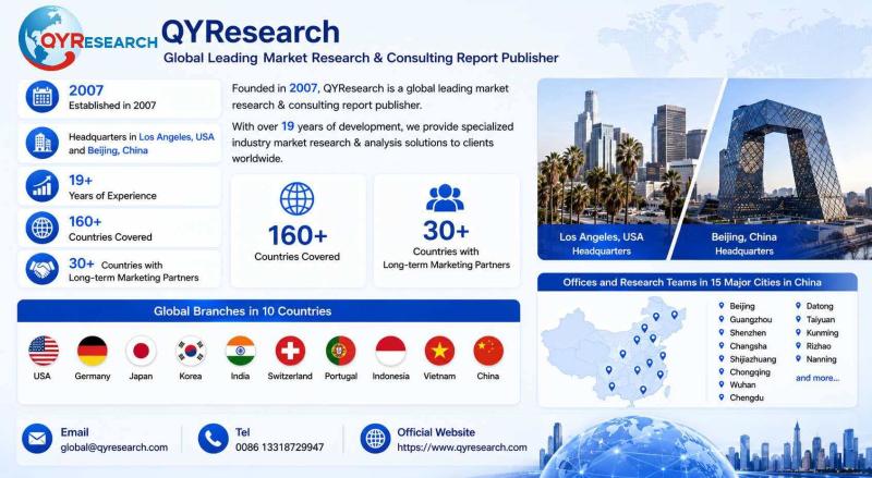
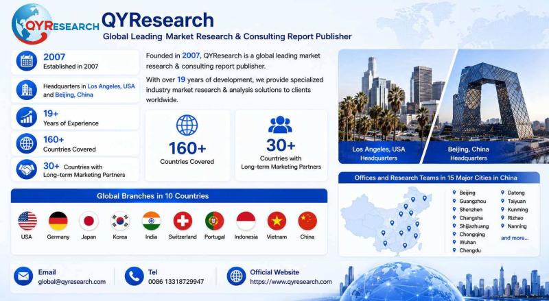
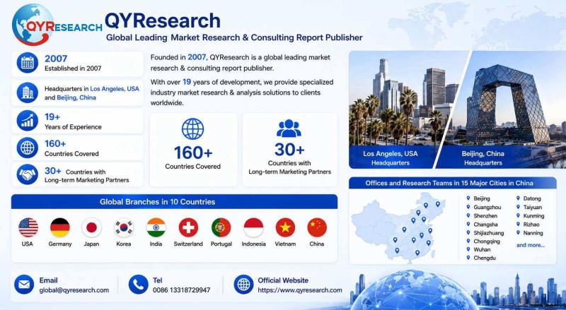
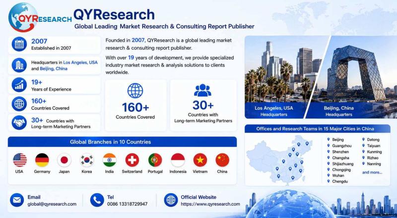
QYResearch founded in California, USA in 2007, which is a leading global market research and consulting company. Our primary business include market research reports, custom reports, commissioned research, IPO consultancy, business plans, etc. With over 19 years of experience and a dedicated research team, we are well placed to provide useful information and data for your business, and we have established offices in 7 countries (include United States, Germany, Switzerland, Japan, Korea, China and India) and business partners in over 30 countries. We have provided industrial information services to more than 60,000 companies in over the world.
Contact Us:
If you have any queries regarding this report or if you would like further information, please contact us:
QY Research Inc.
Add: 17890 Castleton Street Suite 369 City of Industry CA 91748 United States
EN: https://www.qyresearch.com
E-mail: global@qyresearch.com
Tel: 001-626-842-1666(US)
JP: https://www.qyresearch.co.jp
This release was published on openPR.
Permanent link to this press release:
Copy
Please set a link in the press area of your homepage to this press release on openPR. openPR disclaims liability for any content contained in this release.
You can edit or delete your press release Global mSAP Substrate Market Outlook: High-Density Interconnect, Semiconductor Packaging, and AI Infrastructure Growth here
News-ID: 4451449 • Views: …
More Releases from QY Research Inc.
Keyless Bluetooth Car Key Research:market size is projected to reach USD 2.48 bi …
The global market for Keyless Bluetooth Car Key was estimated to be worth US$ 867 million in 2025 and is projected to reach US$ 2481 million, growing at a CAGR of 16.1% from 2026 to 2032.
Global Market Research Publisher QYResearch (QY Research) announces the release of its latest report "Keyless Bluetooth Car Key - Global Market Share and Ranking, Overall Sales and Demand Forecast 2026-2032". Based on 2025 market situation…
Industrial Protocol Conversion Gateway Integration Service Research:CAGR of 6.8% …
The global market for Industrial Protocol Conversion Gateway Integration Service was estimated to be worth US$ 2950 million in 2025 and is projected to reach US$ 4676 million, growing at a CAGR of 6.8% from 2026 to 2032.
Global Market Research Publisher QYResearch (QY Research) announces the release of its latest report "Industrial Protocol Conversion Gateway Integration Service - Global Market Share and Ranking, Overall Sales and Demand Forecast 2026-2032". Based…
Industrial Ammonia Catalyst Research:CAGR of 4.0% during 2026-2032
The global market for Industrial Ammonia Catalyst was estimated to be worth US$ 188 million in 2025 and is projected to reach US$ 246 million, growing at a CAGR of 4.0% from 2026 to 2032.
Global Market Research Publisher QYResearch (QY Research) announces the release of its latest report "Industrial Ammonia Catalyst - Global Market Share and Ranking, Overall Sales and Demand Forecast 2026-2032". Based on 2025 market situation and impact…
HPP Juice Research: CAGR of 7.6% during the forecast period
The global market for HPP Juice was estimated to be worth US$ 1639 million in 2025 and is projected to reach US$ 2864 million, growing at a CAGR of 8.6% from 2026 to 2032.
Global Market Research Publisher QYResearch (QY Research) announces the release of its latest report "HPP Juice - Global Market Share and Ranking, Overall Sales and Demand Forecast 2026-2032". Based on 2025 market situation and impact historical analysis…
More Releases for Substrate
Ceramic Substrate Market
Ceramic Substrate Market Insights
USD 8.4 billion
USD 12.5 billion
5.5%
The Ceramic Substrate Market is witnessing significant growth as the adoption of artificial intelligence expands across industries. The market is expected to register a strong CAGR during the forecast period, driven by the increasing use of machine learning models, autonomous technologies, and advanced analytics. Industries such as healthcare, automotive, retail, financial services, and technology are investing in high-quality training datasets to improve AI…
Diamond Substrate Market to Surge at 11.4% CAGR Through 2033 | Key Players: Crys …
According to a new study by DataHorizzon Research, the Diamond Substrate Market is projected to grow at a CAGR of 11.4% from 2025 to 2033. This exceptional expansion is driven by accelerating adoption of diamond as a next-generation semiconductor substrate material for power electronics, radio frequency devices, and quantum computing applications - sectors where diamond's unmatched combination of thermal conductivity, electrical breakdown strength, and carrier mobility delivers device performance characteristics…
HTCC Ceramic Substrate Market
HTCC Ceramic Substrate Market Overview
HTCC Substrate means High Temperature Co-fired Ceramics Substrate, that is a kind of multilayer ceramic substrate obtained by co-firing a ceramic with a metal pattern such as tungsten or molybdenum which as a high melting point property. Generally, the fired temperature of HTCC substrate is 1500 to 1600 C. HTCC substrate provides the properties of high strength, good heat dissipation, high reliability. The technology is also…
Gallium Nitride Wafer Substrate Market
Gallium Nitride Wafer Substrate Market Overview
Gallium Nitride Wafer Substrate is a high-quality single-crystal substrate. It is made with original HVPE method and wafer processing technology, which has been originally developed for many years. The features are high crystalline, good uniformity, and superior surface quality.
This report provides a deep insight into the global Gallium Nitride Wafer Substrate market covering all its essential aspects. This ranges from a macro overview of the…
Embedded Substrate (ETS) Market
Embedded Substrate (ETS) Market Overview
Embedded Substrate technology is the inclusion of at least one active or passive electrical component within the conductive layers of a substrate, which is a planar structure composed of multiple conductive and insulating layers. Using this technology, it is possible to reduce size, to increase power density, and to improve performance.
This report provides a deep insight into the global Embedded Substrate (ETS) market covering all its…
Ceramic Substrate Market Research Report
The global Ceramic Substrate market was valued at US$ 759 million in 2022 and is anticipated to reach US$ 3022 million by 2029, witnessing a CAGR of 20.1% during the forecast period 2023-2029.
This report studies the metallized ceramic substrates, covers the DBC ceramic substrates, DPC ceramic substrates, AMB ceramic substrates and others. The main ceramic materials are Al2O3, AlN, and SiN.
The influence of COVID-19 and the Russia-Ukraine War were considered…

