Press release
Gallium Nitride Wafer Substrate Market

Gallium Nitride Wafer Substrate is a high-quality single-crystal substrate. It is made with original HVPE method and wafer processing technology, which has been originally developed for many years. The features are high crystalline, good uniformity, and superior surface quality.
This report provides a deep insight into the global Gallium Nitride Wafer Substrate market covering all its essential aspects. This ranges from a macro overview of the market to micro details of the market size, competitive landscape, development trend, niche market, key market drivers and challenges, SWOT analysis, value chain analysis, etc.
In a word, this report is a must-read for industry players, investors, researchers, consultants, business strategists, and all those who have any kind of stake or are planning to foray into the Gallium Nitride Wafer Substrate market in any manner.
To Read Full Market Report-
https://semiconductorinsight.com/report/gallium-nitride-wafer-substrate-market/
Gallium Nitride Wafer Substrate Market Analysis:
The global Gallium Nitride Wafer Substrate market size was estimated at USD 4826.70 million in 2023 and is projected to reach USD 8294.13 million by 2032, exhibiting a CAGR of 6.20% during the forecast period.
North America Gallium Nitride Wafer Substrate market size was estimated at USD 1394.93 million in 2023, at a CAGR of 5.31% during the forecast period of 2025 through 2032.
Gallium Nitride Wafer Substrate Key Market Trends :
Rising Demand in Consumer Electronics
The increasing use of Gallium Nitride (GaN) wafers in smartphones, laptops, and other consumer electronics is driving market growth.
Expansion in Electric Vehicles (EVs)
GaN technology is gaining traction in the EV industry due to its high efficiency and power-saving capabilities.
Advancements in Semiconductor Manufacturing
Innovations in wafer processing and HVPE methods are improving the performance and cost-effectiveness of GaN substrates.
Growing Adoption in Aerospace & Defense
The high-power handling capability of GaN makes it a preferred choice for radar and satellite communication systems.
Increasing Investments in R&D
Major industry players are investing in research and development to enhance GaN wafer efficiency and reduce manufacturing costs.
Download Free Sample Report-
https://semiconductorinsight.com/download-sample-report/?product_id=76771
Gallium Nitride Wafer Substrate Market Regional Analysis :
semi insight
North America:
Strong demand driven by EVs, 5G infrastructure, and renewable energy, with the U.S. leading the market.
Europe:
Growth fueled by automotive electrification, renewable energy, and strong regulatory support, with Germany as a key player.
Asia-Pacific:
Dominates the market due to large-scale manufacturing in China and Japan, with growing demand from EVs, 5G, and semiconductors.
South America:
Emerging market, driven by renewable energy and EV adoption, with Brazil leading growth.
Middle East & Africa:
Gradual growth, mainly due to investments in renewable energy and EV infrastructure, with Saudi Arabia and UAE as key contributors.
Gallium Nitride Wafer Substrate Market Segmentation :
The research report includes specific segments by region (country), manufacturers, Type, and Application. Market segmentation creates subsets of a market based on product type, end-user or application, Geographic, and other factors. By understanding the market segments, the decision-maker can leverage this targeting in the product, sales, and marketing strategies. Market segments can power your product development cycles by informing how you create product offerings for different segments.
Key Company
SCIOCS Corporation
MSE Supplies
Nitride Semiconductors Corporation
Mitsubishi Chemical Corporation
Powdec K K
IQE
Soitec Pte Ltd
Fujitsu Limited
NGK Insulators
Infineon Technologies
LumiGNtech
American Elements
Toshiba
Koninklijke Philips
Texas Instruments
Saint Gobain
Sumitomo Electric Industries
Sino Nitride Semiconductors
Xiamen Powerway Advanced Material
Shanghai Famous Trade Corporation
Market Segmentation (by Type)
4-inch
6-inch
8-inch
Others
Market Segmentation (by Application)
Automobiles
Consumer Electronics
Defense and Aerospace
Industrial Control
Others
Download Free Sample Report-
https://semiconductorinsight.com/download-sample-report/?product_id=76771
FAQs
Q: What are the key driving factors and opportunities in the Gallium Nitride Wafer Substrate market?
A: The rising demand for high-performance semiconductors, 5G expansion, and energy-efficient electronics are key drivers. Opportunities include growth in renewable energy and autonomous vehicles.
Q: Which region is projected to have the largest market share?
A: The Asia-Pacific region, particularly China, Japan, and South Korea, is expected to dominate due to strong semiconductor manufacturing capabilities.
Q: Who are the top players in the global Gallium Nitride Wafer Substrate market?
A: Major companies include SCIOCS Corporation, Mitsubishi Chemical Corporation, Infineon Technologies, Sumitomo Electric Industries, and Texas Instruments.
Q: What are the latest technological advancements in the industry?
A: Advancements include improved HVPE methods, high-purity GaN substrates, and integration of GaN in power electronics and 5G infrastructure.
Q: What is the current size of the global Gallium Nitride Wafer Substrate market?
A: The market was valued at USD 4826.70 million in 2023 and is projected to reach USD 8294.13 million by 2032, with a CAGR of 6.20%.
Other Related Market Reports-
https://sites.google.com/view/semiconductor-insight-2025/e-waste-disposal-market
https://sites.google.com/view/semiconductor-insight-2025/electrostatic-chuck-for-semiconductor-equipment-market
https://sites.google.com/view/semiconductor-insight-2025/elevator-proximity-sensors-market
https://sites.google.com/view/semiconductor-insight-2025/embedded-sim-ic-market
https://sites.google.com/view/semiconductor-insight-2025/quartz-crystal-device-market
https://sites.google.com/view/semiconductor-insight-2025/embedded-substrate-ets-market
https://sites.google.com/view/semiconductor-insight-2025/emi-suppression-capacitor-market
https://sites.google.com/view/semiconductor-insight-2025/emergency-lighting-control-units-market
https://sites.google.com/view/semiconductor-insight-2025/eml-electro-absorption-modulated-laser-market
CONTACT US:
+91 8087992013
City vista, 203A, Fountain Road, Ashoka Nagar, Kharadi, Pune, Maharashtra 411014
About Semiconductor Insight:
Established in 2016, Semiconductor Insight specializes in providing comprehensive semiconductor industry research and analysis to support businesses in making well-informed decisions within this dynamic and fast-paced sector. From the beginning, we have been committed to delivering in-depth semiconductor market research, identifying key trends, opportunities, and challenges shaping the global semiconductor industry.
This release was published on openPR.
Permanent link to this press release:
Copy
Please set a link in the press area of your homepage to this press release on openPR. openPR disclaims liability for any content contained in this release.
You can edit or delete your press release Gallium Nitride Wafer Substrate Market here
News-ID: 3967049 • Views: …
More Releases from semiconductorinsight
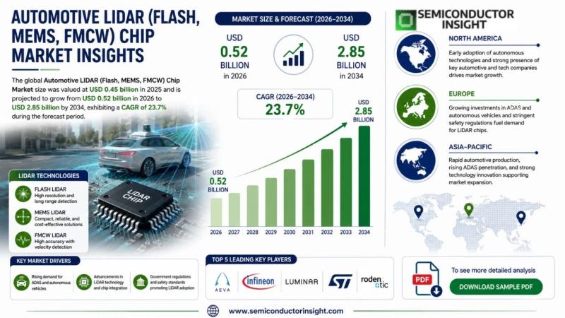
Automotive LiDAR (Flash, MEMS & FMCW) Chip Market to Hit USD 2.85 Billion by 203 …
The global Automotive LIDAR (Flash, MEMS, FMCW) Chip Market, valued at a robust US$ 320 million in 2024, is on a trajectory of significant expansion, projected to reach US$ 1,450 million by 2032. This growth, representing a compound annual growth rate (CAGR) of 20.8%, is detailed in a comprehensive new report published by Semiconductor Insight. The study highlights the critical role of these specialized semiconductor solutions in enabling high-resolution, real-time…
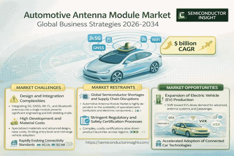
Automotive Antenna Module Market to Reach USD 1.86 Billion by 2032, Growing at 3 …
MARKET INSIGHTS
Global Automotive Antenna Module Market was valued at USD 1.5 billion in 2024 to USD 1.86 billion by 2032, exhibiting a CAGR of 3.6% during the forecast period.
Download Sample Report PDF https://semiconductorinsight.com/download-sample-report/?product_id=122468
Automotive antenna modules are electrical components designed for vehicle mounting that receive and transmit information signals. These systems consist of metallic conductor elements connected to receivers or transmitters via transmission lines. When current flows through the antenna,…

Logic Technology (Foundry) Market
Logic Technology (Foundry) Market Analysis:
The global Logic Technology (Foundry) Market size was estimated at USD 83250 million in 2023 and is projected to reach USD 131941.98 million by 2030, exhibiting a CAGR of 6.80% during the forecast period.
North America Logic Technology (Foundry) market size was USD 21692.57 million in 2023, at a CAGR of 5.83% during the forecast period of 2025 through 2030.
To Read Full Market Report -
https://semiconductorinsight.com/report/logic-technology-foundry-market/
Logic Technology (Foundry)…

Wafer Specialty Technology Foundry Market
Wafer Specialty Technology Foundry Market Analysis:
The global Wafer Specialty Technology Foundry Market size was estimated at USD 45250 million in 2023 and is projected to reach USD 67591.22 million by 2030, exhibiting a CAGR of 5.90% during the forecast period.
North America Wafer Specialty Technology Foundry market size was USD 11790.86 million in 2023, at a CAGR of 5.06% during the forecast period of 2025 through 2030.
To Read Full Market Report…
More Releases for Nitride
Gallium Nitride on Diamond Market
Gallium Nitride on Diamond Market Overview
Gallium nitride-on-Diamond technology is a pioneering materials invention from Akash co-founder, Felix Ejeckam that is created by lifting GaN thin films from its original growth substrate and transferring it to a synthetic CVD diamond substrate which, at 1,600-2,000 W/mK, exhibits the highest known thermal conductivity (4+ times higher than the next best materials) ever manufactured. Bringing together the GaN thin films the core materials…
Europe Silicon Nitride and Silicon Nitride Ceramics Market | Exploring Growth Po …
"In-depth analysis of Silicon Nitride and Silicon Nitride Ceramics Market Overview by 2025-2032
The Silicon Nitride and Silicon Nitride Ceramics Market and Competitive Landscape Highlights - 2025 research report is a comprehensive and invaluable resource for industry professionals and stakeholders. Latest Silicon Nitride and Silicon Nitride Ceramics Market Analysis - 2025-2032. The analysis includes market size, upstream situation, market segmentation, price & cost and industry environment. In addition, the report outlines…
Silicon Nitride and Silicon Nitride Ceramics Market Report: Key Players, Regiona …
LOS ANGELES, United States: QY Research offers an encyclopedic study of the global Silicon Nitride and Silicon Nitride Ceramics market with holistic insights into vital factors and aspects that impact future market growth. The global Silicon Nitride and Silicon Nitride Ceramics market has been analyzed for the forecast period . In order to help players to gain comprehensive understanding of the global Silicon Nitride and Silicon Nitride Ceramics market and its…
Global Silicon Nitride and Silicon Nitride Ceramics Market to Witness a Pronounc …
New report published by Market Research Report Store (MRRS) which offers insights on the global Silicon Nitride and Silicon Nitride Ceramics market.
Click to view the full report TOC, figure and tables:
https://www.marketresearchreportstore.com/reports/294198/global-silicon-nitride-silicon-nitride-ceramics
Global Silicon Nitride and Silicon Nitride Ceramics Market: Forecast by Type / Application / Region
Silicon nitride ceramics offer high thermal, shock, and impact resistance. Silicon nitride ceramics is superior to other materials due to its thermal shock resistance. It does…
Silicon Nitride and Silicon Nitride Ceramics Market, Share, Development forecast …
New report published by Global Info Research which offers insights on the Global Silicon Nitride and Silicon Nitride Ceramics market.
Silicon nitride ceramics offer high thermal, shock, and impact resistance. Silicon nitride ceramics is superior to other materials due to its thermal shock resistance. It does not deteriorate at high temperatures, so it’s used for automotive engines and parts for gas turbines, including the turbocharger rotor. It is widely used in…
