Press release
Patterning Material Industry Trends and key Insights by 2023

Patterning uses the procedure of photolithography and optical masks to reproduce patterns that control the deposition or removal of material from the wafer at specific steps in the device assembly process.Patterning materials are primarily used in semiconductor and automotive industries. Patterning is used in microelectronic devices, automotive sensors, and glass printed circuit boards.Ithas reduced the size of transistors, thus making modern electronic devices affordable.Currently, majority of electronic devices are fabricated using photolithography techniques that depend on sophisticated instrumentation and tailored materials.Patterning materials consist ofspin-on-carbon layers, G line resist, I-line resist, top coat/barrier layer, positive 248nm resist,positive 193nm Immersion resist, positive 193nm dry resist, I-line BARC, 193nm BARC, 248nm BARC, and spin-on-silicon layers.
Get PDF Brochure for more Professional and Technical insights :
http://www.transparencymarketresearch.com/sample/sample.php?flag=B&rep_id=7715
The semiconductor industry is growing at a rapid rate, especially in emerging economies of Asia Pacific. Growth in the semiconductor industry is expected to increase demand for nanodevices and boost demand for patterning material technology. Additionally, rising demand for miniaturized components and development of nanotechnology areanticipated to propel demand for patterning material technology and instruments. Semiconductor manufacturers are establishing production plants in emerging economies of Asia Pacific due to availability of cheap labor and land and government subsidies. However, patterning material technology is expensive as compared to conventional technology. This is likely to hamper growth of the market in the near future.Developing economies are anticipated to offer potential opportunities due to strong demand for electronic products such as tablets and mobile phones during the forecast period.
Asia Pacific, Europe, and North America account for majority share of the patterning materials market. North America is projected to be the largest market for patterning materials followed by Asia Pacific. The U.S. is expected to be the largest market in North America due to presence of large number of end-user industries. Taiwan, China, India, Hong Kong, Australia, New Zealand, South Korea, Japan, Vietnam, Malaysia, and Indonesia are anticipated to be major markets in Asia Pacific.In addition, AsiaPacific is the projected to be the fastest-growing patterning material market as packaging of semiconductors,consumer demand, and production of electronics systems has shifted to this region. The patterning material market in Europe is anticipated to expand at a sluggish rate due to ongoing Eurozone economic crisis.
The market is dominated by large and medium technology and electronic manufacturing companies. Key players operating in this market include JSR Micro, Inc. (the U.S.), DongjinSemichem Co., Ltd. (China), Honeywell Electronic Materials, Inc. (the U.S.), Shin-Etsu Chemical Co., Ltd.(Japan), The DowChemical Company (the U.S.), Applied Materials, Inc.(the U.S.), Tokyo Ohka Kogyo Co., Ltd. (Japan), Sumitomo Chemicals Co., Ltd. (Japan), Merck KGaA(Germany), Microchem Corporation (the U.S.) and Brewer Science, Inc. (the U.S.). Companies are using strategic acquisitions and mergers to remain competitive in the market.
In addition, companies are trying to maintain an elaborate and consistent distribution network, which would allow themto cater to the globalmarket. Furthermore, companies collaborate with each other to develop new and innovative patterning material technology and instruments for end-user industries. In November 2014, Applied Materials, Inc. collaborated with Samsung Electronics Co., Ltd. and PSK Inc., a Korea-based leader in photoresist removal, to produce an advanced patterning solution for fabrication of future generations of NAND and DRAM device designs.
This research report analyzes this market on the basis of its market segments, major geographies, and current market trends.
Geographies analyzed under this research report include
North America
Asia Pacific
Europe
Middle East and Africa
Latin America
This report provides comprehensive analysis of
Market growth drivers
Factors limiting market growth
Current market trends
Market structure
Market projections for upcoming years
About Us
Transparency Market Research (TMR) is a market intelligence company, providing global business information reports and services. Our exclusive blend of quantitative forecasting and trends analysis provides forward-looking insight for thousands of decision makers. TMR's experienced team of Analysts, Researchers, and Consultants, use proprietary data sources and various tools and techniques to gather and analyze information.
Our data repository is continuously updated and revised by a team of research experts, so that it always reflects the latest trends and information. With a broad research and analysis capability, Transparency Market Research employs rigorous primary and secondary research techniques in developing distinctive data sets and research material for business reports.
Contact Us
Transparency Market Research
90 State Street, Suite 700
Albany, NY 12207
Tel: +1-518-618-1030
USA - Canada Toll Free: 866-552-3453
Email: sales@transparencymarketresearch.com
Website: http://www.transparencymarketresearch.com/
This release was published on openPR.
Permanent link to this press release:
Copy
Please set a link in the press area of your homepage to this press release on openPR. openPR disclaims liability for any content contained in this release.
You can edit or delete your press release Patterning Material Industry Trends and key Insights by 2023 here
News-ID: 435020 • Views: …
More Releases from Transparency Market Research
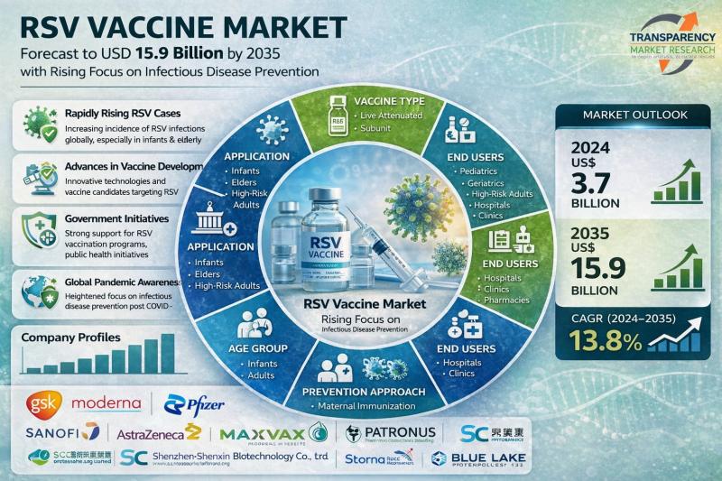
RSV Vaccine Market Size Forecast to USD 15.9 Billion by 2035 with Rising Focus o …
Respiratory Syncytial Virus Vaccine Market Outlook 2035
The global respiratory syncytial virus (RSV) vaccine market was valued at US$ 3.7 Bn in 2024 and is projected to cross US$ 15.9 Bn by the end of 2035, expanding at a CAGR of 13.8% from 2025 to 2035. The market is witnessing rapid growth driven by increasing awareness of RSV infections, rising immunization programs, and strong pipeline developments by leading pharmaceutical companies.
👉 Get…
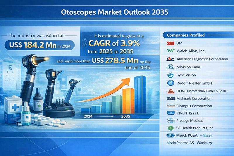
Otoscopes Market Outlook 2035: Digital Innovation, Rising Ear Disorder Cases, an …
The global otoscopes market was valued at US$ 184.2 Mn in 2024 and is projected to expand at a compound annual growth rate (CAGR) of 3.9% from 2025 to 2035, reaching more than US$ 278.5 Mn by the end of 2035. This steady growth trajectory reflects the increasing demand for advanced diagnostic tools, rising awareness of ear health, and continuous technological advancements in medical devices.
The market's moderate yet consistent expansion…
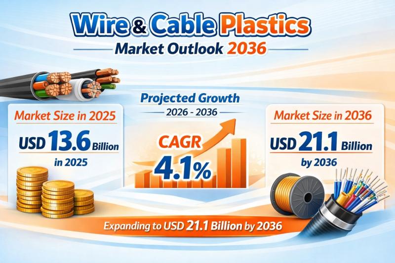
Wire & Cable Plastics Market to Reach USD 21.1 Billion by 2036 - Expanding at 4. …
The global Wire & Cable Plastics Market was valued at USD 13.6 Billion in 2025 and is projected to reach USD 21.1 Billion by 2036, growing at a compound annual growth rate (CAGR) of 4.1% from 2026 to 2036.
Access key findings and insights from our Report in this sample -
https://www.transparencymarketresearch.com/sample/sample.php?flag=S&rep_id=65801
This steady growth reflects the increasing importance of advanced polymer compounds in electrical infrastructure, telecommunications, renewable energy systems, and emerging digital…
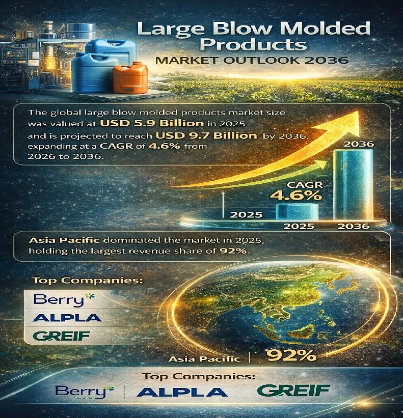
Large Blow Molded Products Market to Reach USD 9.7 Billion by 2036 Driven by Ris …
The global large blow molded products market is witnessing steady growth, driven by increasing demand for lightweight, durable, and cost-effective plastic products across various industries. The market size was valued at USD 5.9 Billion in 2025 and is projected to reach USD 9.7 Billion by 2036, expanding at a CAGR of 4.6% from 2026 to 2036. Growing applications in packaging, automotive, construction, and industrial sectors are significantly contributing to market…
More Releases for Patterning
Global Patterning Materials Market, Size, Trends, Business Strategies 2025-2032
Patterning Materials Market Overview
Patterning is the backbone of scaling, which has reduced the size of the transistor to where it is today, in turn making modern electronic devices increasingly affordable. This report analzyed the materials for patterning. This report provides a deep insight into the global Patterning Materials market covering all its essential aspects. This ranges from a macro overview of the market to micro details of the market size,…
Laser Patterning Equipment Market Size, Share, Development by 2024
LP INFORMATION offers a latest published report on Laser Patterning Equipment Market Analysis and Forecast 2019-2025 delivering key insights and providing a competitive advantage to clients through a detailed report.
According to this study, over the next five years the Laser Patterning Equipment market will register a xx% CAGR in terms of revenue, the global market size will reach US$ xx million by 2024, from US$ xx million in 2019.…
Laser Patterning Equipment Market Size, Share, Development by 2025
Market Research Report Store offers a latest published report on Laser Patterning Equipment Market Analysis and Forecast 2019-2025 delivering key insights and providing a competitive advantage to clients through a detailed report.
The Laser Patterning Equipment market was valued at xx Million US$ in 2018 and is projected to reach xx Million US$ by 2025, at a CAGR of xx% during the forecast period. In this study, 2018 has been considered…
Patterning Material Market Latest Report with Forecast 2016 – 2024
The global market for patterning materials is poised to register a steady growth rate over the course of the forecast period, fueled by the numerous applications they are used in. The emerging, yet highly lucrative, market for nanodevices is a key factor boosting the demand for patterning materials, along with an expanding integrated circuit market.
Read Report Overview @
https://www.transparencymarketresearch.com/patterning-material-market.html
The report identifies the major driving and restraining forces that impact the…
Patterning Material Market - Global Industry Analysis 2024 | Research report
Global Patterning Material Market: Overview
The global market for patterning materials is poised to register a steady growth rate over the course of the forecast period, fueled by the numerous applications they are used in. The emerging, yet highly lucrative, market for nanodevices is a key factor boosting the demand for patterning materials, along with an expanding integrated circuit market.
Browse Market Research Report @
http://www.transparencymarketresearch.com/patterning-material-market.html
The report identifies the major…
Patterning Material Market - Global Industry Analysis 2023
Patterning uses the procedure of photolithography and optical masks to reproduce patterns that control the deposition or removal of material from the wafer at specific steps in the device assembly process.Patterning materials are primarily used in semiconductor and automotive industries. Patterning is used in microelectronic devices, automotive sensors, and glass printed circuit boards.Ithas reduced the size of transistors, thus making modern electronic devices affordable.Currently, majority of electronic devices are fabricated…
