Press release
E-Beam Wafer Inspection System Market is Expected to Progress at a CAGR of 18.3% to Reach US$ 4,630.3 Million by 2035
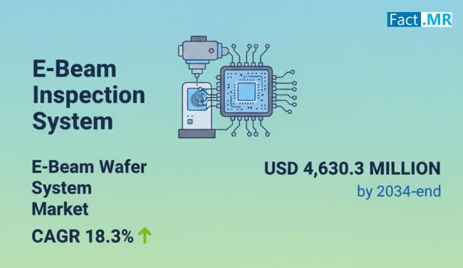
E-Beam Wafer Inspection System Market
E-beam wafer inspection systems are ideal for their ability to provide ultra-high-resolution nanoscale defect detection, down to 1-2 nanometers, enabling precise identification of surface and subsurface defects. This capability is critical for the semiconductor industry, where even minor defects can significantly impact the performance, yield, and reliability of electronic devices such as microprocessors, memory chips, and advanced integrated circuits.
For More Insights into the Market, Request a Sample of this Report:
https://www.factmr.com/connectus/sample?flag=S&rep_id=8011
Market Segmentation and Insights
The e-beam wafer inspection system market can be segmented by technology, wafer size compatibility, application, and region. Advanced e-beam inspection systems utilize electron microscopy, scanning electron beam, and high-resolution imaging technology to detect defects such as contamination, pattern irregularities, and micro-cracks. These systems are increasingly integrated with automated defect classification and data analytics software to enable real-time quality control and process optimization in semiconductor fabrication.
By wafer size, systems supporting 200 mm and 300 mm wafers dominate the market, aligning with standard semiconductor production lines. Emerging applications for 450 mm wafers are being explored in research and high-volume manufacturing, particularly for next-generation electronics, 5G devices, and AI processors. The ability to inspect larger wafers with precision is becoming a key differentiator among manufacturers, as larger wafers reduce production costs while maintaining high-quality output.
By application, e-beam wafer inspection systems are utilized extensively in semiconductor fabrication, research & development, and quality assurance operations. Semiconductor manufacturers use these systems to detect and classify nanoscale defects before wafer processing, improving yield rates and reducing. R&D institutions employ e-beam inspection systems to innovate new materials, circuits, and nanoscale devices, supporting the advancement of emerging technologies such as quantum computing, AI chips, and high-performance electronics.
Regional Insights
North America leads the e-beam wafer inspection system market, driven by the presence of advanced semiconductor manufacturers, research facilities, and a strong focus on innovation. Europe follows, supported by investments in semiconductor fabrication and R&D infrastructure. The Asia-Pacific region is emerging as the fastest-growing market due to increasing semiconductor manufacturing activities in countries like Taiwan, South Korea, Japan, and China. These regions are investing heavily in advanced inspection systems to maintain global competitiveness and meet the growing demand for electronics in consumer, industrial, and automotive sectors.
Browse Full Report: https://www.factmr.com/report/e-beam-wafer-inspection-system-market
Recent Developments and Key Players
The e-beam wafer inspection system market is highly competitive, with key players including Applied Materials, KLA Corporation, Hitachi High-Technologies, ASML, JEOL, and Advantest. Companies are focusing on product innovation, software integration, and automation to provide higher accuracy, faster throughput, and improved reliability.
Recent developments include the launch of next-generation e-beam inspection systems with enhanced resolution, faster scanning speeds, and AI-driven defect recognition. For example, KLA Corporation introduced an advanced e-beam inspection system capable of detecting sub-nanometer defects while integrating cloud-based analytics for real-time process monitoring. Hitachi High-Technologies enhanced its wafer inspection systems with improved signal-to-noise ratio and advanced imaging software, enabling higher precision in semiconductor defect detection.
Strategic collaborations, acquisitions, and partnerships are also shaping the competitive landscape. Companies are partnering with semiconductor fabs and R&D labs to co-develop inspection technologies that address evolving industry needs. Startups focusing on nanoscale inspection innovations are attracting investments, further intensifying competition and accelerating technological advancements in the market.
Conclusion
The e-beam wafer inspection system market is poised for significant growth over the next decade, driven by the rising demand for defect-free semiconductor wafers, technological innovation, and expanding semiconductor fabrication activities globally. With high-resolution capabilities, automation, and AI integration, e-beam inspection systems are becoming indispensable tools in semiconductor manufacturing and R&D. Leading manufacturers and emerging startups have substantial opportunities to capitalize on the growing need for precision, efficiency, and reliability in the semiconductor industry from 2025 to 2035.
Check out More Related Studies Published by Fact.MR:
Hydraulic Gear Pump Market
https://www.factmr.com/report/2991/hydraulic-gear-pump-market
Load Monitoring Systems Market
https://www.factmr.com/report/2996/load-monitoring-systems-market
Blanking Machine Market
https://www.factmr.com/report/3040/blanking-machine-market
Excavator Augers Market
https://www.factmr.com/report/3041/excavator-augers-market
Contact:
US Sales Office
11140 Rockville Pike
Suite 400
Rockville, MD 20852
United States
Tel: +1 (628) 251-1583, +353-1-4434-232
Email: sales@factmr.com
About Fact.MR
We are a trusted research partner of 80% of fortune 1000 companies across the globe. We are consistently growing in the field of market research with more than 1000 reports published every year. The dedicated team of 400-plus analysts and consultants is committed to achieving the utmost level of our client's satisfaction.
This release was published on openPR.
Permanent link to this press release:
Copy
Please set a link in the press area of your homepage to this press release on openPR. openPR disclaims liability for any content contained in this release.
You can edit or delete your press release E-Beam Wafer Inspection System Market is Expected to Progress at a CAGR of 18.3% to Reach US$ 4,630.3 Million by 2035 here
News-ID: 4173316 • Views: …
More Releases from Fact.MR
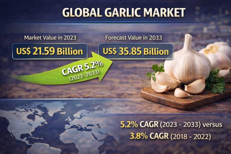
Garlic Market to Reach USD 35.85B by 2033 at 5.2% CAGR Led by California Garlic …
The global garlic market is projected to grow from USD 21.59 billion in 2023 to USD 35.85 billion by 2033, expanding at a CAGR of 5.2%. Growth is driven by increasing demand for garlic in culinary applications, health-focused diets, and processed food industries worldwide.
Get Detailed Market Forecasts, Competitive Benchmarking, and Pricing Trends: https://www.factmr.com/connectus/sample?flag=S&rep_id=303
📊 Quick Stats at a Glance
Market Size (2023): USD 21.59 Billion
Forecast Value (2033): USD 35.85 Billion
CAGR (2023-2033): 5.2%
Historical…
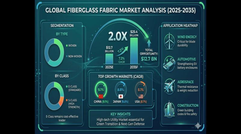
Global Fiberglass Fabric Market to Surpass USD 25.4 Billion by 2035; Wind Energy …
According to a comprehensive market analysis by Fact.MR, the industry is projected to grow from USD 11.8 billion in 2024 to USD 25.4 billion by 2035, expanding at a steady CAGR of 7.2%.The global fiberglass fabric market is undergoing a structural shift as industries pivot toward high-performance, lightweight, and fire-resistant materials.
Get detailed market forecasts, competitive benchmarking, and pricing trends
https://www.factmr.com/connectus/sample?flag=S&rep_id=878
This growth is anchored by the dual imperatives of decarbonization and…
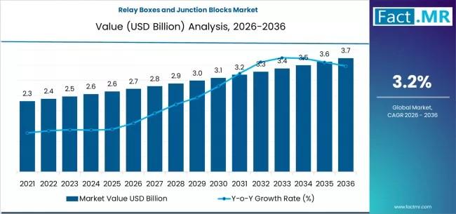
Relay Boxes and Junction Blocks Market to Reach USD 3.63 billion by 2036, Driven …
The global relay boxes and junction blocks market is entering a pivotal expansion phase as industries accelerate the transition toward complex electrical architectures. According to the latest market analysis by Fact.MR, the market is valued at USD 2.72 billion in 2026 and is projected to reach USD 3.63 billion by 2036, expanding at a steady CAGR of 3.2%.
This growth reflects a structural transformation in power distribution strategies, where robust management…
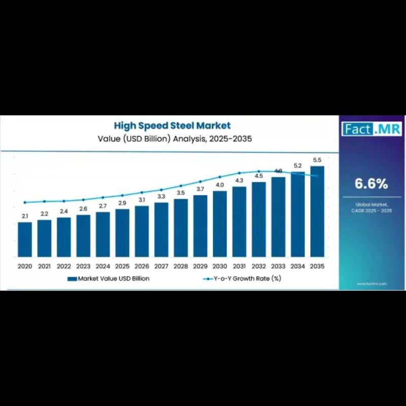
Global High Speed Steel Market to Reach USD 5.5 Billion by 2035, Driven by Preci …
According to a comprehensive market study by Fact.MR, the global high speed steel market is projected to grow from USD 2.9 billion in 2025 to USD 5.5 billion by 2035, expanding at a steady CAGR of 6.6%.As industrial automation and high-precision manufacturing redefine the global production landscape, the high speed steel (HSS) market is undergoing a significant technological transformation.
Get detailed market forecasts, competitive benchmarking, and pricing trends
https://www.factmr.com/connectus/sample?flag=S&rep_id=883
The surge is…
More Releases for Wafer
Wafer Surface Thinning Machine Market 2026-2032: Fully Automatic Wafer Grinders, …
Global Leading Market Research Publisher QYResearch announces the release of its latest report "Wafer Surface Thinning Machine - Global Market Share and Ranking, Overall Sales and Demand Forecast 2026-2032". For semiconductor fabs, OSATs (outsourced semiconductor assembly and test providers), and institutional investors tracking advanced packaging, the wafer back-grinding process has emerged as a critical bottleneck and differentiator. As 3D stacking, fan-out wafer-level packaging (FOWLP), and power device miniaturization intensify, the…
Semiconductor Silicon Wafer Market Is Going to Boom |• Silicon Wafer • Globa …
Worldwide Market Reports has released a new in-depth research study on the "Semiconductor Silicon Wafer Market," highlighting strong growth potential in the coming years. The report delivers a structured and data-driven analysis of the market landscape, combining robust research methodology, market sizing, validated data modeling, and insights sourced from reliable primary and secondary channels.
The study thoroughly examines key market aspects, including growth drivers, restraints, challenges, emerging opportunities, technological advancements, innovation…
Wafer Hybrid Bonding Equipment Market Share Driven by Wafer-to-Wafer Technology …
Wafer Hybrid Bonding Equipment Market Size
The global market for Wafer Hybrid Bonding Equipment was valued at US$ 164 million in the year 2024 and is projected to reach a revised size of US$ 756 million by 2031, growing at a CAGR of 24.7% during the forecast period.
View sample report
https://reports.valuates.com/request/sample/QYRE-Auto-31W14822/Global_Wafer_Hybrid_Bonding_Equipment_Market_Insights_Forecast_to_2029
The Wafer Hybrid Bonding Equipment market is experiencing accelerated growth, driven by increasing demand for advanced semiconductor packaging technologies that enable higher…
Semiconductor Wafer Electrostatic Chucks for 300mm Wafer Market
Semiconductor Wafer Electrostatic Chucks for 300mm Wafer Market
The global Semiconductor Wafer Electrostatic Chucks for 300mm Wafer market was valued at US$ 1165 million in 2023 and is anticipated to reach US$ 1672.7 million by 2030, witnessing a CAGR of 5.3% during the forecast period 2024-2030.
View Sample Report
https://reports.valuates.com/request/sample/QYRE-Auto-38F13137/Global_Semiconductor_Wafer_Electrostatic_Chucks_for_300mm_Wafer_Market_Research_Report_2023
Report Scope
The Semiconductor Wafer Electrostatic Chucks for 300mm Wafer market size, estimations, and forecasts are provided in terms of output/shipments (Units) and revenue…
Automatic Mounter Wafer Equipment Market Report 2018: Segmentation by Type (100 …
Global Automatic Mounter Wafer Equipment market research report provides company profile for Lintec Corporation, Nitto Denko, Tokyo Electron, Technovision, Takatori, Ultron Systems, DISCO Corp., Syagrus Systems, Advanced Dicing Technologies, Longhill Industries and Others.
This market study includes data about consumer perspective, comprehensive analysis, statistics, market share, company performances (Stocks), historical analysis 2012 to 2017, market forecast 2018 to 2025 in terms of volume, revenue, YOY growth rate, and CAGR for…
EMEA Solar Wafer Cutting Fluid PEG Market For Semiconductor, Solar Wafer, Crysta …
Latest industry research report on: EMEA (Europe, Middle East and Africa) Solar Wafer Cutting Fluid PEG Market : Industry Size, Share, Research, Reviews, Analysis, Strategies, Demand, Growth, Segmentation, Parameters, Forecasts
Request For Sample Report @ https://www.marketresearchreports.biz/sample/sample/1194694
Geographically, this report split EMEA into Europe, the Middle East and Africa, With sales (K MT), revenue (Million USD), market share and growth rate of Solar Wafer Cutting Fluid PEG for these regions, from 2012 to…
