Press release
3D TSV Packages Market Set for Strong 15.1% CAGR Growth Through 2035

3D TSV Packages Market
Get Sample Report: - https://www.futuremarketinsights.com/reports/sample/rep-gb-1398
The 3D TSV package market is paying significant attention as advanced packaging technologies continue to reopen the semiconductor landscape. The Three-Dynamical Through-Silicon via (3D TSV) packaging is a revolutionary technology used to stack silicon vertically with high density interconnects. This enables better electrical performance, small form factors and low power consumption - in the required amounts in modern electronic devices. Consumer electronics, automotive systems and data centers demand rapidly high performance and energy-skilled components, the importance of 3D TSV technology is more pronounced than ever.
The 3D TSV package is characterized by rapid innovation in the market and increasing implementation in a wide range of industries. This packaging technique allows for rapid data processing, low delay and better bandwidth, making it an indispensable part of the next generation computing and communication systems. With exponential increase in data consumption and the spread of AI, IOT, and 5G network, the market is ready to expand rapidly in the coming years.
Market Trends
A major trend that shapes the 3D TSV package market is an infection towards asymmetrical integration. Maker can get significant benefits in functionality and performance, by dying many types of logic, memory and sensors in the same package. This change is encouraging more companies to adopt 3D TSV packaging in an attempt to maintain with the law of Moore through system-level innovations rather than traditional scaling.
Another remarkable trend is the growing cooperation between semiconderies Founders and Integrated device manufacturers (IDMs). These partnerships are designed to streamline production processes, reduce costs and expedite the market from time to time. Additionally, the increase in wearable equipment, AR/VR technology and autonomous vehicles has created new applications that greatly rely more on compactness and performance benefits introduced by 3D TSV packaging.
Driving Forces Behind Market Growth
Many factors are increasing the development of the 3D TSV package market. One of the primary catalysts is the increasing demand for small and high-demonstration electronic devices. Smartphones, tablets, and wearbals all require compact and efficient semiconductor solutions. High interconnect density and short interconnect length of 3D TSV packages make them ideal for such applications.
The increase in investment in high-demonstration computing (HPC) and data centers is another powerful driver. With the expansion of cloud computing and AI-operated applications, data centers require a continuous requirement of chips that can handle large-scale data throughput with minimal delay. The use of 3D TSV packaging helps to meet these stringent performance requirements, leading to further market expansion.
In addition, the deployment of advanced semiconductor solutions is accelerating by increasing 5G technology. 5G base stations and user devices require components that support rapid data transmission and low power consumption. These requirements are well informed by 3D TSV technology, making it a favorite option among telecommunications tool manufacturers.
Challenges and Opportunities
Despite its promising development trajectory, the 3D TSV package faces many challenges in the market. One of the major concerns is the high cost of production. Complex construction processes involved in creating 3D TSVs, including wafer thinning, contribute to advanced manufacturing costs, through carvings, and bonding. These cost factors can widely limit adoption, especially between small and medium -sized enterprises.
Thermal management is another important challenge. Khadi standing with several layers of dying, heat dissipation becomes a matter of concern. If not properly managed, thermal issues can affect devices reliability and performance. Engineers are actively working on the novel cooling technology and thermal interface material to solve the issue.
On the other hand, these challenges also open doors for innovation and development. Companies with specialization in advanced materials, thermal solutions and manufacturing equipment can capitalize to capitalize on the demand for cost -effective and efficient solutions. Additionally, educational research and industrial R&D lead to innovations that can potentially reduce manufacturing complexity and improve yield rates.
Explore In-Depth Analysis-Click Here to Access the Report:- https://www.futuremarketinsights.com/reports/3d-tsv-packages-market
Recent Industry Developments
• 3D TSV package market has done many notable development in recent times. Companies are rapidly launching products with integrated 3D TSV technology to meet the increasing demand for high speed and low-distraction devices. For example, memory manufacturers are now producing high-bandwidth memory (HBM) solutions that take advantage of 3D TSV architecture to give better performance in data-intensive applications.
• In addition, semiconductor equipment manufacturers have introduced the next generation equipment designed specifically for TSV formation and inspection. This progression is improving manufacturing precision, reducing defects, and the production of production is increasing. In addition, industry cooperation is leading to standardization of TSV processes, further enhances scalability and compatibility in various platforms.
• The increasing presence of government -backed initiatives to promote domestic semiconductor production is also positively affecting the market. Many countries have launched programs aimed at strengthening their semiconductor ecosystems, providing financial assistance and encouragement to adopt advanced packaging technologies such as 3D TSVs.
Regional Analysis
Geographically, the 3D TSV package market displays different degrees of development and adoption in different fields. The Asia-Pacific dominates the global landscape, roughly due to the presence of major semiconductor manufacturers in countries such as Taiwan, South Korea, Japan and China. These countries have invested heavy in research and development, construction facilities and supply chain integration, making the region a center for advanced packaging technologies.
North America is an important part of the market, inspired by technological innovation and strong demand from industries such as aerospace, defense and high-demonstrations. The field benefits from the presence of major chip designers and strong cooperation between academics and industry.
Europe is also emerging as a promising market, which focuses on increased investment in semiconductor research and increasing industrial automation and motor vehicle electronics. The area's emphasis on energy efficiency and smart manufacturing aligns well with the benefits introduced by 3D TSV packaging.
Competitive Outlook
The competitive landscape of the 3D TSV package market is marked by a mixture of installed players and innovative startups. These companies are engaged in fierce competition to increase their product offerings and expand their market share. R&D expenses, strategic partnership, and merger and acquisition are employed to gain a competitive edge.
Major industry players are making heavy investments in developing scalable 3D TSV solutions that can be adapted for various applications. Attention is on improving yield, reducing costs and increasing performance. Additionally, companies are rapidly collaborating with end-users to co-develop applications that align application-specific solutions that align with industry needs.
Startups and small firms are also making their mark by presenting top solutions addressing specific challenges within the 3D TSV ecosystem. Focusing on their agility and innovation allows them to rapidly adapt to market dynamics and customer requirements.
Top Companies
Several key players are at the forefront of the 3D TSV packages market. These include semiconductor giants like Intel, TSMC, Samsung Electronics, and ASE Group. These companies have vast experience and technical capabilities in developing advanced packaging solutions, including 3D TSV technology.
Other noteworthy participants include Amkor Technology, STATS ChipPAC, and JCET Group. These firms are known for their robust packaging services and global customer base. Additionally, equipment suppliers such as Applied Materials and Lam Research play a critical role in providing the tools and technologies necessary for TSV fabrication and integration.
The market also includes innovative players such as Xperi Corporation and Tezzaron Semiconductor, which are exploring new approaches to TSV design and integration. Their contributions are helping to broaden the scope of applications and push the boundaries of what's possible with 3D TSV technology.
Segmentation Outlook
By Process Realization:
• By process realization, the industry is classified into via first, via middle, and via last segments.
By Application:
• By application, the industry is divided into logic & memory devices, MEMS & sensors, and power & analog components.
By End Users:
• The industry caters to multiple industries, including consumer electronics, information & communication technologies, automotive, military & defense, aerospace, and medical sectors.
By Region:
• The industry spans key global regions, including North America, Latin America, Europe, Asia Pacific, and the Middle East & Africa.
Semiconductors Industry Analysis Reports: -
Fiber Optic Gyroscope Market Size and Share Forecast Outlook 2025 to 2035
https://www.futuremarketinsights.com/reports/fiber-optics-gyroscope-market
Embedded Hypervisor Market Size, Share, and Demand Forecast 2025 to 2035
https://www.futuremarketinsights.com/reports/embedded-hypervisor-market
I2C Bus Market Size, Share, and Forecast Outlook from 2025 to 2035
https://www.futuremarketinsights.com/reports/i2c-bus-market
Wide Bandgap Semiconductors Market Outlook 2025 to 2035
https://www.futuremarketinsights.com/reports/wide-bandgap-semiconductors-market
Coaxial Cable Market Outlook 2025 to 2035
https://www.futuremarketinsights.com/reports/coaxial-cable-market
Future Market Insights Inc.
Christiana Corporate, 200 Continental Drive,
Suite 401, Newark, Delaware - 19713, USA
T: +1-347-918-3531
For Sales Enquiries: sales@futuremarketinsights.com
Website: https://www.futuremarketinsights.com
Future Market Insights, Inc. (ESOMAR certified, recipient of the Stevie Award, and a member of the Greater New York Chamber of Commerce) offers profound insights into the driving factors that are boosting demand in the market. FMI stands as the leading global provider of market intelligence, advisory services, consulting, and events for the Packaging, Food and Beverage, Consumer Technology, Healthcare, Industrial, and Chemicals markets. With a vast team of over 400 analystsworldwide, FMI provides global, regional, and local expertise on diverse domains and industry trends across more than 110 countries.
This release was published on openPR.
Permanent link to this press release:
Copy
Please set a link in the press area of your homepage to this press release on openPR. openPR disclaims liability for any content contained in this release.
You can edit or delete your press release 3D TSV Packages Market Set for Strong 15.1% CAGR Growth Through 2035 here
News-ID: 4039337 • Views: …
More Releases from Future Market Insights

Easy Peel Film Market to Reach USD 164.3 Billion by 2035 | Top Key Players: Berr …
The Easy Peel Film Market is estimated at USD 87.5 billion in 2025 and is projected to reach USD 164.3 billion by 2035, expanding at a CAGR of 6.5% during the forecast period. Growth is being fueled by rising demand for convenient, tamper-evident, and shelf-life-extending packaging across food, beverage, pharmaceutical, and consumer goods sectors.
As packaging becomes a core differentiator in competitive retail environments, the Easy Peel Film Market is evolving…
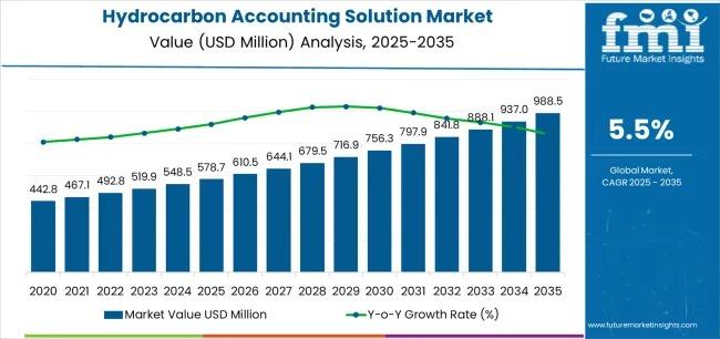
Hydrocarbon Accounting Solution Market Set to Reach USD 988.4 Million by 2035 as …
The global hydrocarbon accounting solution market is projected to expand from USD 578.7 million in 2025 to USD 988.4 million by 2035, registering a steady compound annual growth rate (CAGR) of 5.5%. This expansion reflects a structural shift across the oil and gas industry toward digital platforms capable of delivering accurate production allocation, automated reconciliation, and regulatory compliance in increasingly complex operational environments. As production portfolios expand across unconventional resources,…
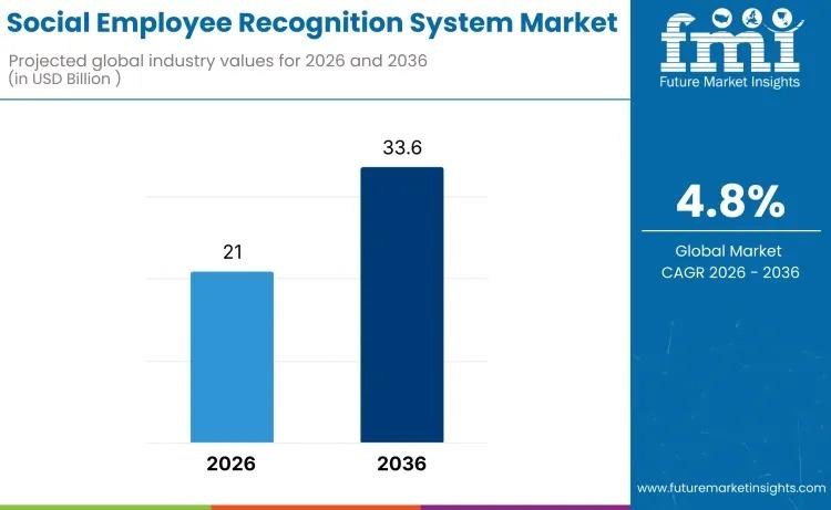
Social Employee Recognition System Market to Reach USD 33.6 Billion by 2036 as D …
The global social employee recognition system market is entering a new phase of strategic expansion, projected to grow from USD 21.0 billion in 2026 to USD 33.6 billion by 2036, reflecting a compound annual growth rate (CAGR) of 4.8%. This sustained growth trajectory highlights the increasing importance of employee engagement technologies in shaping organizational culture, enhancing workforce productivity, and supporting talent retention initiatives across diverse industries.
Organizations worldwide are prioritizing digital…
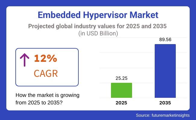
Embedded Hypervisor Market Set for Strong Expansion as Software-Defined Vehicles …
The global embedded hypervisor market is entering a period of accelerated expansion, driven by rising adoption of software-defined architectures across automotive, aerospace, industrial automation, and telecommunications industries. The market is projected to grow from USD 25.25 billion in 2025 to USD 89.56 billion by 2035, advancing at a compound annual growth rate (CAGR) of 12%, reflecting the increasing importance of secure, high-performance virtualization in mission-critical embedded systems.
Embedded hypervisors-specialized software layers…
More Releases for TSV
TSV Electroplating Additive Market Size, Growth Opportunities and Forecast 2025- …
Los Angeles, United State: A newly published report titled "Global TSV Electroplating Additive Market Insights, Forecast to 2025-2031" by QY Research throws light on the industry dynamics and current and future trends that play a key role in determining the business expansion. The global TSV Electroplating Additive market was valued at US$ 224 million in 2024 and is anticipated to reach US$ 372 million by 2031, witnessing a CAGR of…
Through Silicon Via (TSV) Technology Market 2022 | Detailed Report
The Through Silicon Via (TSV) Technology report compiles the market information depending upon market development and growth factors, optimizing the growth path. In addition, it highlights the strategies and market share of the leading vendors in the particular market. The report follows a robust research methodology model that helps to make informed decisions. It obtains both qualitative and quantitative market information supported by primary research.
The Through Silicon Via (TSV) Technology…
Through Silicon Via (TSV) Technology Market 2021 | Detailed Report
Global Through Silicon Via (TSV) Technology Market 2021-2027, has been prepared based on an in-depth market analysis with inputs from industry experts. The report covers the market landscape and its growth prospects in the coming years. The report includes a discussion of the key vendors operating in this market. An exclusive data offered in this report is collected by research and industry experts team.
Get Free Sample PDF (including full TOC,…
3D TSV and 2.5D Market Size, Share, Development by 2024
Market Research Report Store offers a latest published report on 3D TSV and 2.5D Market Analysis and Forecast 2019-2025 delivering key insights and providing a competitive advantage to clients through a detailed report.
The global 3D TSV and 2.5D market is valued at xx million USD in 2018 and is expected to reach xx million USD by the end of 2024, growing at a CAGR of xx% between 2019 and 2024.
The…
Global 3D TSV Market Share and Growth 2019 - QY Research
3D TSV is a vertical electrical connection (via) that passes completely through a silicon wafer or die. TSVs are high performance interconnect techniques used as an alternative to wire-bond and flip chips to create 3D packages and 3D integrated circuits. Compared to alternatives such as package-on-package, the interconnect and device density is substantially higher, and the length of the connections becomes shorter.
The global 3D TSV market is valued at xx…
3D TSV Packages Market Value Chain and Forecast 2016-2026
Currently, 3D Packaging using Through Silicon Via technology (3D TSV) is one of the hottest topics in the semiconductor ecosystem. 3D TSV is vertical electrical connection (via) passing completely through a silicon wafer or die. These short vertical interconnects are replacing the long interconnects of 2D packaging technologies including wire-bond and flip chips.
Growing demand for high density and multifunctional microelectronics with improved performance, and the reduction of timing delays is…
