Press release
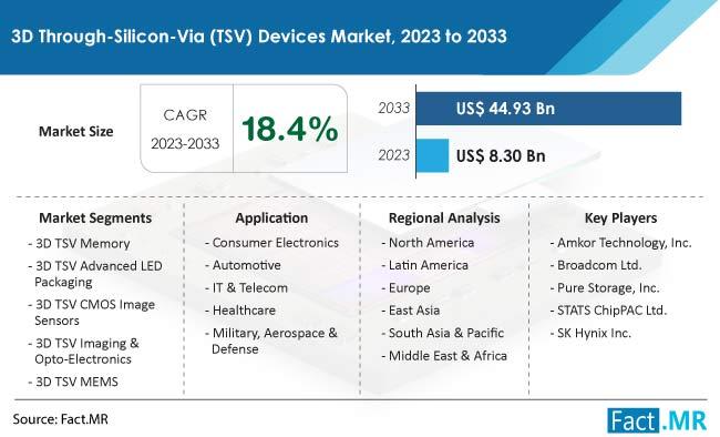
3D Through-Silicon-Via (TSV) Devices Market is Projected to Reach US$ 44.93 Billion by 2033
3D Through-Silicon-Via (TSV) Devices Market
3D TSV solutions are a type of packaging technology used in the semiconductor industry to vertically stack and interconnect multiple integrated circuit (IC) chips. TSV technology is a crucial advancement that enables the integration of three-dimensional (3D) silicon and 3D integrated circuits (ICs). It facilitates the shortest interconnections between chips and allows for the interconnection of smaller pad sizes and pitches. The stacking of chips in a three-dimensional arrangement using TSV technology has become an emerging and advanced packaging solution for memories, CMOS imagers, and MEMS.
For More Insights into the Market, Request a Sample of this Report:
https://www.factmr.com/connectus/sample?flag=S&rep_id=6959
Key Segments of 3D Through-Silicon-Via (TSV) Devices Industry Research Report
By Product : 3D TSV Memory, 3D TSV Advanced LED Packaging, 3D TSV CMOS Image Sensors, 3D TSV Imaging & Opto-Electronics, 3D TSV MEMS
By Process Realization : First Process Realization, Middle Process Realization, Last Process Realization
By Application : Consumer Electronics, Automotive, IT & Telecom, Healthcare, Military, Aerospace, & Defense
By Region : North America, Latin America, Europe, East Asia, South Asia & Oceania, MEA
TSV devices also lower power consumption due to shorter interconnects and improved heat dissipation. They support the integration of diverse technologies and materials, improving reliability.
The growth of the 3D Through-Silicon-Via (TSV) devices market is primarily driven by the increasing demand for compact and high-performance electronic devices. As consumers and industries seek smaller, more powerful gadgets, the TSV technology enables enhanced integration density and improved performance.
Implementing 3D Through-Silicon-Via (TSV) technology is challenging due to complex manufacturing processes like etching, bonding, and thinning. Etching involves precisely creating vertical vias, bonding requires accurate layer connections, and thinning reduces wafer thickness. Stacking multiple layers of devices in a small space can result in heat dissipation challenges, requiring effective thermal management solutions to prevent overheating.
Browse Full Report with TOC@ https://www.factmr.com/report/3d-through-silicon-via-tsv-devices-market
Key Takeaways:
The United States market is expected to witness a CAGR of 18.9% during the forecast period (2023-2033). Moreover, the UK market is predicted to witness a market value of US $ 2.74 Bn in 2033. India and China market is predicted to witness a value of US $ 3.7 Bn and US $ 8.13 Bn by 2033 respectively.
The German market for 3D TSV devices is valued at US $ 614.1 Mn in 2023.
Increasing investments in semiconductor manufacturing initiatives are expected to contribute to the sales of devices in China. China's market is expected to reach a market value of US $ 8.13 Bn by 2033.
Market Competition
In this competitive market, major stakeholders are dedicated to advancing 3D Through-Silicon Via (TSV) technologies, including cutting-edge packaging solutions, increased interconnect densities, and improved power efficiency. Notable companies at the forefront of these developments include Amkor Technology, Inc., Broadcom Ltd., Pure Storage, Inc., STATS ChipPAC Ltd., SK Hynix Inc., and Invensas Corporation.
In a noteworthy advancement in June 2022, Intel achieved progress in power management for chipsets within 3D stacked System in Package (SIP) designs. The company introduced fully integrated voltage regulators (FIVRs) incorporating embedded inductors.
Leading companies in the market are engaging with strategic partnerships and collaborations with other key companies including system integrators, device manufacturers, and semiconductor manufacturers.
Winning strategies
Major players in the 3D through-silicon-via (TSV) devices market is smartly focusing on creating advanced packaging solutions. These solutions use 3D TSV technology to tackle specific challenges in high-performance computing, mobile devices, and automotive electronics.'
Given the importance of memory in various electronic devices, key players might emphasize strategies that involve the vertical stacking of memory components using 3D TSV technology, catering to the demand for high-capacity and high-performance memory solutions.
As the demand for smaller and more energy-efficient devices grows in wearables and IoT, key players in the market should focus on strategies that highlight the benefits of making devices smaller. 3D TSV technology enables compact and integrated devices without compromising performance, ideal for sleek wearables.
Get Customization on this Report for Specific Research Solutions:
https://www.factmr.com/connectus/sample?flag=RC&rep_id=6959
The adoption of 3D TSV devices in consumer electronics is anticipated to experience a Compound Annual Growth Rate (CAGR) of 18.6% over the next decade.
Manufacturers of consumer electronics are actively pursuing the development of smaller, slimmer, and more compact devices. The use of 3D Through-Silicon Via (TSV) technology enables the vertical integration of components, leading to increased device density and a smaller overall footprint. By eliminating the need for traditional wire bonding or flip-chip interconnects, TSV devices contribute to significant size reduction, making them well-suited for portable devices like smartphones, tablets, wearables, and various other electronic gadgets.
Consumers now demand advanced features and capabilities from their electronic devices. 3D TSV devices play a crucial role in meeting these expectations by facilitating improved functionality through the integration of diverse components-such as processors, memory chips, sensors, and communication modules-into a single package. This integrated approach enhances device performance, supports multi-functional capabilities, and contributes to seamless user experiences.
About Fact.MR:
We are a trusted research partner of 80% of fortune 1000 companies across the globe. We are consistently growing in the field of market research with more than 1000 reports published every year. The dedicated team of 400-plus analysts and consultants is committed to achieving the utmost level of our client's satisfaction.
Contact:
US Sales Office
11140 Rockville Pike
Suite 400
Rockville, MD 20852
United States
Tel: +1 (628) 251-1583, +353-1-4434-232 (D)
Sales Team: sales@factmr.com
This release was published on openPR.
Permanent link to this press release:
Copy
Please set a link in the press area of your homepage to this press release on openPR. openPR disclaims liability for any content contained in this release.
You can edit or delete your press release 3D Through-Silicon-Via (TSV) Devices Market is Projected to Reach US$ 44.93 Billion by 2033 here
News-ID: 3561917 • Views: …
More Releases from Fact.MR
Snacks Market is Growing at USD 569.2 billion in 2025 | Fact.MR Report
The global snacks market is projected to grow from USD 545.2 billion in 2026 to approximately USD 835.4 billion by 2036. This growth reflects a steady compound annual growth rate (CAGR) of 4.3% over the ten-year forecast period. The market is being fundamentally reshaped by the "snackification" of meals, where busy consumers are increasingly replacing traditional breakfast, lunch, and dinner with portable, nutrient-dense snacking options.
Get Access of Report Sample: https://www.factmr.com/connectus/sample?flag=S&rep_id=50
Quick…
Liquid Nutritional Supplement Market Growing from USD 42.0 billion in 2025 to US …
The global liquid Nutritional supplements market is projected to grow from USD 33.25 billion in 2026 to approximately USD 45.10 billion by 2036. This growth represents a compound annual growth rate (CAGR) of 6.1% to 10.2% depending on the specific product segment (e.g., high-growth Ready-to-Drink formulations vs. traditional tonics).
The market is being primarily driven by a "pill fatigue" trend among consumers and an aging global population that increasingly prefers…
FMCG Logistics Market is Expected to Hit USD 190.5 billion by 2036 | Fact.MR Ins …
The global FMCG logistics market is projected to grow from USD 126.9 billion in 2026 to approximately USD 189.5 billion by 2036. This growth reflects a steady compound annual growth rate (CAGR) of 4.1% over the ten-year forecast period.
The market is entering a decade of transformation, shifting from a focus on cost-driven efficiency to automation-led resilience as retailers and brands navigate the complexities of quick-commerce and global supply chain…
Bio-Based Ethyl Acrylate Market Forecasted CAGR of 12.6% by 2036 | Fact.MR Repor …
The global Bio-Based Ethyl Acrylate Market is projected to expand significantly over the next decade as demand for sustainable, performance-oriented monomers rises across coatings, adhesives, textiles, and specialty chemical applications. Industry analysts estimate that the market, valued at approximately USD 450 million in 2025, is expected to reach around USD 940 million by 2035, representing a compound annual growth rate (CAGR) of about 7.9% over the forecast period.
Get Access of…
More Releases for TSV
TSV Electroplating Additive Market Size, Growth Opportunities and Forecast 2025- …
Los Angeles, United State: A newly published report titled "Global TSV Electroplating Additive Market Insights, Forecast to 2025-2031" by QY Research throws light on the industry dynamics and current and future trends that play a key role in determining the business expansion. The global TSV Electroplating Additive market was valued at US$ 224 million in 2024 and is anticipated to reach US$ 372 million by 2031, witnessing a CAGR of…
Through Silicon Via (TSV) Technology Market 2022 | Detailed Report
The Through Silicon Via (TSV) Technology report compiles the market information depending upon market development and growth factors, optimizing the growth path. In addition, it highlights the strategies and market share of the leading vendors in the particular market. The report follows a robust research methodology model that helps to make informed decisions. It obtains both qualitative and quantitative market information supported by primary research.
The Through Silicon Via (TSV) Technology…
Through Silicon Via (TSV) Technology Market 2021 | Detailed Report
Global Through Silicon Via (TSV) Technology Market 2021-2027, has been prepared based on an in-depth market analysis with inputs from industry experts. The report covers the market landscape and its growth prospects in the coming years. The report includes a discussion of the key vendors operating in this market. An exclusive data offered in this report is collected by research and industry experts team.
Get Free Sample PDF (including full TOC,…
3D TSV and 2.5D Market Size, Share, Development by 2024
Market Research Report Store offers a latest published report on 3D TSV and 2.5D Market Analysis and Forecast 2019-2025 delivering key insights and providing a competitive advantage to clients through a detailed report.
The global 3D TSV and 2.5D market is valued at xx million USD in 2018 and is expected to reach xx million USD by the end of 2024, growing at a CAGR of xx% between 2019 and 2024.
The…
Global 3D TSV Market Share and Growth 2019 - QY Research
3D TSV is a vertical electrical connection (via) that passes completely through a silicon wafer or die. TSVs are high performance interconnect techniques used as an alternative to wire-bond and flip chips to create 3D packages and 3D integrated circuits. Compared to alternatives such as package-on-package, the interconnect and device density is substantially higher, and the length of the connections becomes shorter.
The global 3D TSV market is valued at xx…
3D TSV Packages Market Value Chain and Forecast 2016-2026
Currently, 3D Packaging using Through Silicon Via technology (3D TSV) is one of the hottest topics in the semiconductor ecosystem. 3D TSV is vertical electrical connection (via) passing completely through a silicon wafer or die. These short vertical interconnects are replacing the long interconnects of 2D packaging technologies including wire-bond and flip chips.
Growing demand for high density and multifunctional microelectronics with improved performance, and the reduction of timing delays is…
