Press release
Ultra-Precise Additive Manufacturing Enables Serial Production of Micro-Optics
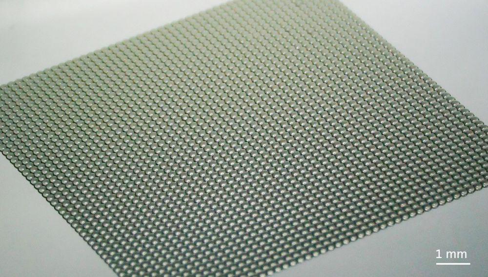
3D printed polymer master of a microlens array
Nanoscribe’s new Photonic Professional GT2 3D printers change the way to produce micro-optical components. This additive manufacturing technology enables the fabrication of ultra-precise micro-optics as polymer masters for serial production, which are needed, for instance, in mobile or augmented reality devices, for sophisticated sensors or advanced solutions in healthcare and automotive industry.
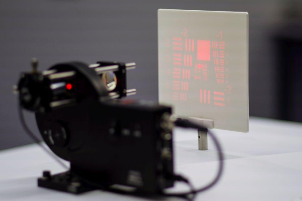
At the upcoming SPIE Photonics West, the leading trade fair in optics and photonics, Nanoscribe presents the entire process chain for series production of micro-optics based on 3D printed polymer masters as starting point (booth 366, South Hall). Up to now, the production of innovative micro-optical designs has been challenging due to very high demands with respect to shape accuracy and low surface roughness required for optimum optical performance. Furthermore, product development processes have to cope with the ever-increasing importance of rapid innovation cycles and low costs for serial production.
Serial Production by Injection Molding
The 3D printed polymer masters fit well into common industrial processes for series production such as injection molding, hot embossing and nanoimprint lithography. For example, a nickel shim is generated by electroforming the 3D printed polymer master of a microlens array. The shim is then used as an insert for injection molding of a thermoplastic polymer, such as PMMA (polymethyl methacrylate) or PC (polycarbonate). Within seconds the molten thermoplastic is injected into the insert cavity, cooled and solidified, duplicating the polymer master shape. This standard process cuts the production time and costs per piece to affordable consumer market products. Other techniques include replication by UV molding of a photosensitive material from PDMS (polydimethylsiloxane) negative stamps. At the upcoming SPIE Photonics West 2019, Nanoscribe presents the replicating production chain of micro-optics by means of injection molding and UV molding.
Additive Manufacturing of Micro-Optics
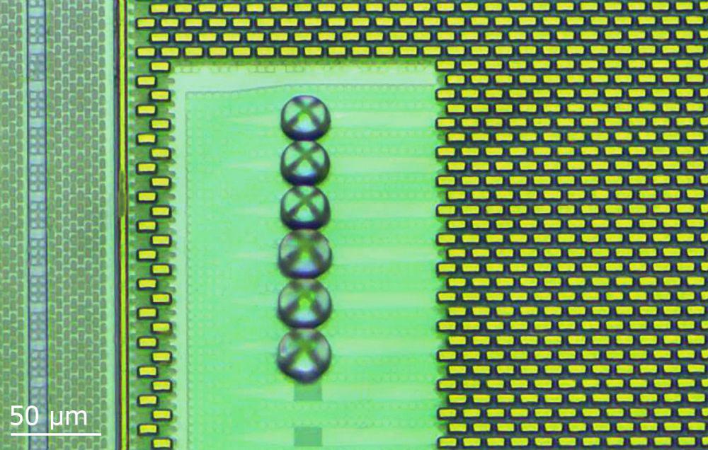
Based on the powerful technology of two-photon polymerization (2PP) Nanoscribe's 3D printers transform digital models directly into physical objects with submicron resolution. In comparison to conventional methods, such as gray-scale lithography, reflow techniques or diamond milling, Nanoscribe's 3D printers provide enormous freedom of design and at the same time a very robust chemical process to produce almost any concave or convex surface shape. Compact refractive optics, such as corner cubes with sharp edges, freeform optics and even compound lens systems of two or more stacked lenses have been produced with this technology. The straightforward workflow from a CAD model to the final 3D printed part contributes to direct and fast design optimization, shortening the product design iteration cycles. Also, multilevel diffractive optical elements with submicron resolution benefit from the one-step printing process that speeds up prototyping and polymer master fabrication at reduced costs, e.g. omitting several lithography steps and mask making.
The high precision 3D printer uses a femtosecond laser beam that exposes and solidifies photosensitive material only in the tight focal point. The printer scans the laser focus within a photoresin in a layer-by-layer fashion with layer distances down to the nanometer scale, creating 3D objects with optical surface quality in a single printing step. The additive process enables the fabrication of micro-optics with designs that are otherwise impossible to produce. Hemispherical and aspherical microlens arrays, for instance, can be fabricated with arbitrarily small distances between the lenses allowing even to overlap the lenses. Furthermore, they show smooth surfaces with a surface roughness of just a few nanometers and a shape accuracy of less than one micrometer. Both regular or computer-designed random lens arrangements can benefit from additive manufacturing, for example, in homogenizer applications required for illumination purposes. The combination of Nanoscribe's advanced processes, software recipes with optimized print parameters and tailor-made 2PP resins is a key advantage for the direct fabrication of high-precision micro-optics, overcoming geometrical constraints known from standard fabrication methods and achieving high shape accuracy and optical smooth surfaces.
About us:
Nanoscribe GmbH, located in Eggenstein-Leopoldshafen near Karlsruhe (Germany), develops and provides 3D printers for microfabrication as well as photoresins and process solutions. Since the foundation in 2007, the company has managed to turn from a spin-off of the Karlsruhe Institute of Technology (KIT, Germany) to a medium-sized company with more than 65 employees. Nanoscribe established itself as a global market- and technology leader for 3D printing on the micro- and mesoscale. Worldwide, more than 1,000 users in top universities and pioneer companies benefit from Nanoscribe´s technology and award-winning solutions for microfabrication.
Nanoscribe GmbH
Hermann-von-Helmholtz-Platz 1
76344 Eggenstein-Leopoldshafen
Germany
www.nanoscribe.com
Media Contact:
Anke Werner
werner@nanoscribe.com
+49 (0)721 981980 501
This release was published on openPR.
Permanent link to this press release:
Copy
Please set a link in the press area of your homepage to this press release on openPR. openPR disclaims liability for any content contained in this release.
You can edit or delete your press release Ultra-Precise Additive Manufacturing Enables Serial Production of Micro-Optics here
News-ID: 1557616 • Views: …
More Releases from Nanoscribe GmbH
Photonic Professional GT2 Prints Diffractive Optical Elements with Submicron Pre …
Nanoscribe presents additively manufactured multi-level DOEs at SPIE Photonics West 2019
At the upcoming Photonics West 2019, the prestigious trade fair for optics and photonics taking place in San Francisco, Nanoscribe showcases multi-level diffractive optical elements (DOEs) that are fabricated by means of high resolution 3D printers Photonic Professional GT2 (Nanoscribe, booth 366, South Hall).
The fabrication of multi-level DOE microstructures gains more and more attention, both in scientific research as well…
On-Chip 3D Microprinting for Photonic and MEMS Systems: Additive manufacturing o …
Growing demands on high-speed data communication, unmanned aerial vehicles and portable medical devices are attracting industries to new manufacturing methods like, for example, Nanoscribe’s direct laser writing technology. Currently, the production of photonic circuits and microelectromechanical systems (MEMS) needed for these applications requires different manufacturing methods and multiple process steps for bringing together various components on one microchip. Now, with Nanoscribe’s highest resolution 3D printers one can print and integrate…
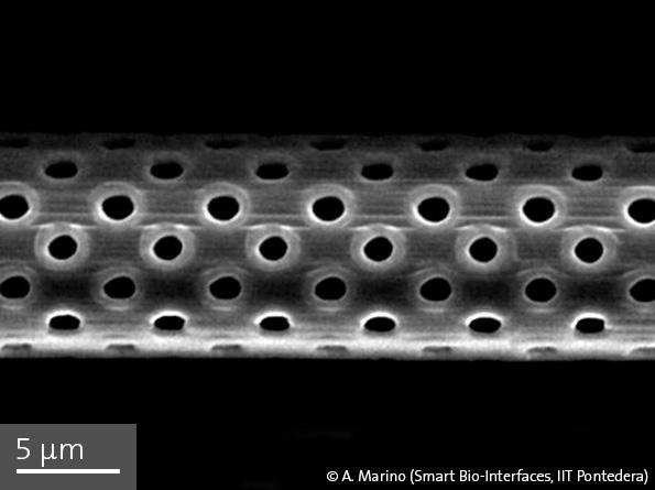
Ultra-Precise 3D Printing Can Help Drug Testing for Treating Brain Disorders
Following you will find pioneering research results from the IIT - Istituto Italiano di Tecnologia (Italian Institute of Technology) recently highlighted on the inside cover of the well-known scientific journal Small:
Researchers of the Smart Bio Interfaces group at the IIT in Pontedera (Pisa, Italy) created the first biohybrid device mimicking the blood-brain barrier by means of a Nanoscribe 3D printer. The understanding of the blood-brain barrier mechanisms is target of…
More Releases for Photonic
Photonic Integrated Circuit Market : An Overview
Introduction:
Photonic Integrated Circuits (PICs) are transforming the landscape of optical communication and processing by integrating multiple photonic functions into a single chip. Unlike traditional electronic circuits that rely on electrical signals, PICs use light (photons) for data transmission, offering unparalleled speed, efficiency, and bandwidth. These circuits are critical in applications such as data centers, telecommunications, healthcare, and defense. With the growing demand for faster and more energy-efficient systems, PICs are…
Photonic Integrated Circuit Market: A Comprehensive Overview
Photonic Integrated Circuits (PICs) represent a revolutionary advancement in the field of optics and electronics. By integrating multiple photonic devices onto a single chip, these circuits facilitate the manipulation of light for various applications, including telecommunications, data communications, sensing, and medical devices. The need for high-speed data transmission and processing has spurred significant interest in PIC technology, resulting in a rapidly expanding market.
Market Size
Data Bridge Market Research analyses that the…
Photonic AI Chip Market 2024 Research Report
Photonic AI Chip Market
A Photonic AI Chip, also known as a photonic processor or optical AI chip, is a specialized integrated circuit that leverages photonics (the science and technology of generating and manipulating photons) to perform AI computations. Instead of relying solely on traditional electronic components, photonic AI chips use light signals to carry out parallel processing and execute machine learning tasks.
The global Photonic AI Chip market was valued at…
Photonic ICs Market Emerging Trends and Company Profiles to Watch-APIC, Infinera …
The Photonic ICs are also known as integrated optoelectronics devices or planer light wave circuits. The rising need for the high transmission capacity of the optical fibers is the primary parameter responsible for the popularity of the photonic ICs in the industry applications. The data generated at the organizational operations is increasing day by day with the globalization of the businesses, with the deployment of photonic ICs in the systems…
Global Photonic Crystal Market 2018 Growth Rate by Players: Palo Alto Research C …
Market Research Store Exposed a new deep Industry research report focuses on Photonic Crystal Market, delivers detailed analysis of market and future prospects of Photonic Crystal market. The critical and significant data in the study makes the research a very important tool for experts, analysts and managers to get ready-to-access analysis by the industry professionals. The Photonic Crystal Market report provides the complete analysis of Photonic Crystal Market Size Data…
Global Photonic Crystal Market Trend Analysis by 2025: Photonic Lattice, Opalux, …
Qyresearchreports include new market research report Global Photonic Crystal Market Professional Survey Report 2018 to its huge collection of research reports.
This report studies the global Photonic Crystal market status and forecast, categorizes the global Photonic Crystal market size (value & volume) by manufacturers, type, application, and region. This report focuses on the top manufacturers in North America, Europe, Japan, China, India, Southeast Asia and other regions (Central & South America,…
