Press release
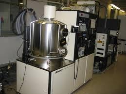
E-Beam Wafer Inspection System Market: Requirement for Superior Quality Semiconductors to Propel the Growth
Request Sample: https://www.transparencymarketresearch.com/sample/sample.php?flag=S&rep_id=15884
According to Transparency Market Research, the global E-beam wafer inspection system market is anticipated to flourish with a strong CAGR of 17.5% during forecast period from 2015 to 2025. ASML Holding N.V. (Netherlands), Hitachi Ltd. (Japan), KLA Tencor Corporation (The U.S.), NXP Semiconductors N.V. (Netherlands), Taiwan Semiconductor Manufacturing Co. Ltd. (Taiwan), Lam Research Corporation (The U.S.), Synopsys Inc. (The U.S.)Integrated Device Technology Inc. (The U.S.), Renesas Electronics Corporation (Japan), and Applied Materials Inc. (The U.S.) are some of the key companies dominating the global E-beam wafer inspection system market. In year 2016, Asia pacific was evaluated to be the most dominant region among all, with 60% of market shares. Based on application, the defect imaging emerged as the largest application segment with a share of 38.5% in the market in year 2016. It is foreseen to remain prevailing through the duration of the forecast period.
Miniaturization to Boost the Global E-Beam Wafer Inspection System Market
Wafers are imperative equipment that are integrated in smaller devices. It is crucial to inspect for faults and defects for these devices to run error-free for quite a while. E-beam inspection system helps in the detection of the any errors or flaws in compact gadgets, for example, smartphones, MEMs, laptops among numerous others. Due to this, with the developing demand for developing miniature versions which are aimed at enhancing the complete performance over several industries, the usage of these wafer inspection systems is expected to rise, along these lines giving stimulating the market. E-beam id cards employed for finding flaws in the voltage-balance alongside minute defects. It further helps in reducing the charging of the wafer surface. These elements are likely to support the progress of the market in the coming years. However, the market may face obstruction from the presence of some alternate inspection gadgets over various regions.
Browse Our Report: https://www.transparencymarketresearch.com/e-beam-wafer-inspection-system-market.html
Demand in Semiconductors Wafers to Support Market Growth
The increase in the appropriation of specialized devices and consumer electronic equipment, for example, tablets, wearables, smartphones, LEDs, LCDs, and SSDs have resulted in the high requirement for superior quality semiconductors, for example, silicon-based wafers. Likewise, the rising fame of several novel and emerging technologies, for example, IoT, M2M, UHD TVs, vehicle robotization, and hybrid laptops is additionally driving the demand for semiconductor wafers. This recent increase in the demand for semiconductor wafers subsequently fosters the need for wafer inspection systems to keep a check on the process and nature of the wafers.
The study presented here is based on a report by Transparency Market Research (TMR), titled, “E-Beam Wafer Inspection System Market (Type - Less Than 1 nm, 1 to 10 nm, and More Than 10 nm; Application - Defect Imaging, Lithographic Qualification, Bare Wafer OQC/IQC, Wafer Dispositioning, Reticle Quality Inspection, and Inspector Recipe Optimization) - Global Industry Analysis, Size, Share, Growth, Trends and Forecast 2017 - 2025.”
Get TOC of This Report: https://www.transparencymarketresearch.com/report-toc/15884
Transparency Market Research (TMR) is a market intelligence company, providing global business information reports and services. Our exclusive blend of quantitative forecasting and trends analysis provides forward-looking insight for thousands of decision makers. TMR’s experienced team of analysts, researchers, and consultants, use proprietary data sources and various tools and techniques to gather, and analyze information. Our business offerings represent the latest and the most reliable information indispensable for businesses to sustain a competitive edge.
US Office
90 State Street, Suite 700
Albany, NY 12207
Tel: +1-518-618-1030
USA - Canada Toll Free: 866-552-3453
Email: sales@transparencymarketresearch.com
Website: https://www.transparencymarketresearch.com
This release was published on openPR.
Permanent link to this press release:
Copy
Please set a link in the press area of your homepage to this press release on openPR. openPR disclaims liability for any content contained in this release.
You can edit or delete your press release E-Beam Wafer Inspection System Market: Requirement for Superior Quality Semiconductors to Propel the Growth here
News-ID: 972742 • Views: …
More Releases from Transparency Market Research
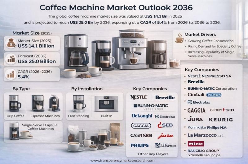
Coffee Machine Market to Reach US$ 25.0 Billion by 2036, Driven by At-Home Premi …
The global coffee machine market was valued at US$ 14.1 Billion in 2025 and is projected to reach US$ 25.0 Billion by 2036, expanding at a CAGR of 5.4% from 2026 to 2036. Market growth is being driven by rising global coffee consumption, increasing demand for premium and specialty coffee at home, busy urban lifestyles, rapid product innovation, smart connectivity features, strong e-commerce penetration, expanding middle-class incomes, compact kitchen trends,…
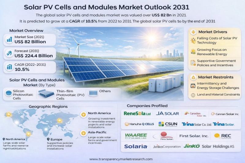
Solar PV Cells and Modules Market to Surpass US$ 224.4 Billion by 2031, Growing …
The global solar PV cells and modules market was valued at over US$ 82 Bn in 2021 and is projected to grow at a robust CAGR of 10.5% from 2022 to 2031. By the end of 2031, the market is expected to cross US$ 224.4 Bn, reflecting the accelerating global transition toward renewable energy sources and sustainable power generation.
Strong policy support, corporate net-zero commitments, and rapid technological advancements in photovoltaic…
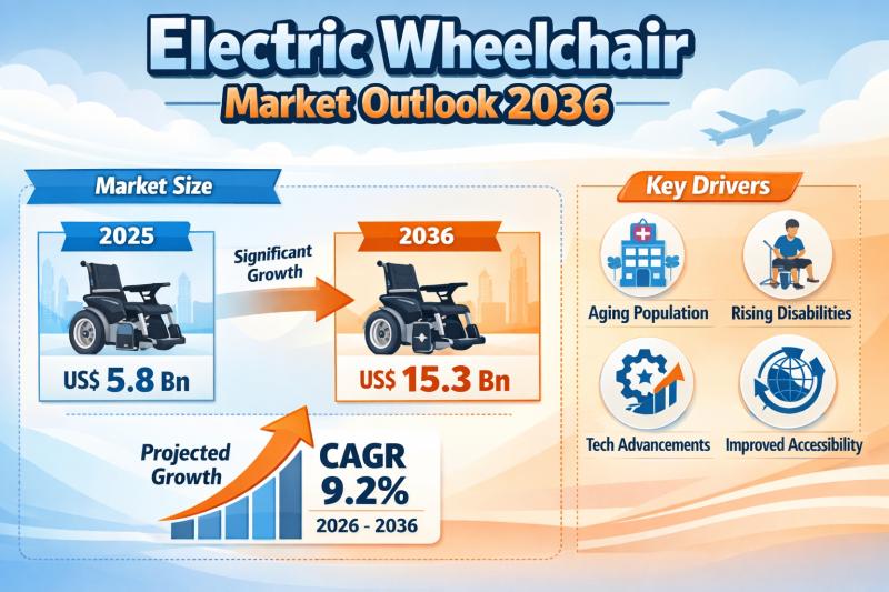
Electric Wheelchair Market Expanding at 9.2% CAGR Through 2036 - By Control Type …
The global electric wheelchair market continues to demonstrate strong and sustained growth, fueled by demographic transitions, technological innovation, and expanding healthcare access worldwide. Valued at US$ 5.8 billion in 2025, the market is projected to reach US$ 15.3 billion by 2036, expanding at a compound annual growth rate (CAGR) of 9.2% from 2026 to 2036.
Discover essential conclusions and data from our Report in this sample -
https://www.transparencymarketresearch.com/sample/sample.php?flag=S&rep_id=4198
This robust trajectory reflects rising…

Vehicle Predictive Maintenance Market Size Forecast to USD 13.7 Billion by 2036 …
Vehicle Predictive Maintenance Market Outlook 2036
The global vehicle predictive maintenance market was valued at USD 3 Billion in 2025 and is projected to reach USD 13.7 Billion by 2036, expanding at a robust CAGR of 14.7% from 2026 to 2036. Market growth is driven by increasing adoption of connected vehicles, rising fleet digitalization, advancements in AI-driven analytics, and growing emphasis on minimizing vehicle downtime and maintenance costs.
👉 Get your sample…
More Releases for Wafer
Semiconductor Silicon Wafer Market Is Going to Boom |• Silicon Wafer • Globa …
Worldwide Market Reports has released a new in-depth research study on the "Semiconductor Silicon Wafer Market," highlighting strong growth potential in the coming years. The report delivers a structured and data-driven analysis of the market landscape, combining robust research methodology, market sizing, validated data modeling, and insights sourced from reliable primary and secondary channels.
The study thoroughly examines key market aspects, including growth drivers, restraints, challenges, emerging opportunities, technological advancements, innovation…
Semiconductor Wafer Electrostatic Chucks for 300mm Wafer Market Size, Trends & F …
Semiconductor Wafer Electrostatic Chucks for 300mm Wafer Market Size
The global Semiconductor Wafer Electrostatic Chucks for 300mm Wafer market is projected to grow from US$ 1227 million in 2024 to US$ 1672.7 million by 2030, at a Compound Annual Growth Rate (CAGR) of 5.3% during the forecast period.
Get Free Sample: https://reports.valuates.com/request/sample/QYRE-Auto-38F13137/Global_Semiconductor_Wafer_Electrostatic_Chucks_for_300mm_Wafer_Market_Research_Report_2023?utm_source=openpr&utm_medium=referral
The US & Canada market for Semiconductor Wafer Electrostatic Chucks for 300mm Wafer is estimated to increase from $ million in…
Wafer Hybrid Bonding Equipment Market Share Driven by Wafer-to-Wafer Technology …
Wafer Hybrid Bonding Equipment Market Size
The global market for Wafer Hybrid Bonding Equipment was valued at US$ 164 million in the year 2024 and is projected to reach a revised size of US$ 756 million by 2031, growing at a CAGR of 24.7% during the forecast period.
View sample report
https://reports.valuates.com/request/sample/QYRE-Auto-31W14822/Global_Wafer_Hybrid_Bonding_Equipment_Market_Insights_Forecast_to_2029
The Wafer Hybrid Bonding Equipment market is experiencing accelerated growth, driven by increasing demand for advanced semiconductor packaging technologies that enable higher…
Semiconductor Wafer Electrostatic Chucks for 300mm Wafer Market
Semiconductor Wafer Electrostatic Chucks for 300mm Wafer Market
The global Semiconductor Wafer Electrostatic Chucks for 300mm Wafer market was valued at US$ 1165 million in 2023 and is anticipated to reach US$ 1672.7 million by 2030, witnessing a CAGR of 5.3% during the forecast period 2024-2030.
View Sample Report
https://reports.valuates.com/request/sample/QYRE-Auto-38F13137/Global_Semiconductor_Wafer_Electrostatic_Chucks_for_300mm_Wafer_Market_Research_Report_2023
Report Scope
The Semiconductor Wafer Electrostatic Chucks for 300mm Wafer market size, estimations, and forecasts are provided in terms of output/shipments (Units) and revenue…
Automatic Mounter Wafer Equipment Market Report 2018: Segmentation by Type (100 …
Global Automatic Mounter Wafer Equipment market research report provides company profile for Lintec Corporation, Nitto Denko, Tokyo Electron, Technovision, Takatori, Ultron Systems, DISCO Corp., Syagrus Systems, Advanced Dicing Technologies, Longhill Industries and Others.
This market study includes data about consumer perspective, comprehensive analysis, statistics, market share, company performances (Stocks), historical analysis 2012 to 2017, market forecast 2018 to 2025 in terms of volume, revenue, YOY growth rate, and CAGR for…
EMEA Solar Wafer Cutting Fluid PEG Market For Semiconductor, Solar Wafer, Crysta …
Latest industry research report on: EMEA (Europe, Middle East and Africa) Solar Wafer Cutting Fluid PEG Market : Industry Size, Share, Research, Reviews, Analysis, Strategies, Demand, Growth, Segmentation, Parameters, Forecasts
Request For Sample Report @ https://www.marketresearchreports.biz/sample/sample/1194694
Geographically, this report split EMEA into Europe, the Middle East and Africa, With sales (K MT), revenue (Million USD), market share and growth rate of Solar Wafer Cutting Fluid PEG for these regions, from 2012 to…
