Press release
Wafer Level Packaging Market Projected to Expand Vigorous By 2026

Packaging industry has made strides in terms of design incorporating functionality into the mix. Innovations in packaging have become key to keeping up with the changing needs of the consumers as well as the manufacturers. Packaging has encompassed almost all the industries in the world and they have individually experienced a shift in their packaging designs. One of the most interesting industries to incorporate packaging innovation into their operations is the semiconductor and technology industry.
Wafer level packaging Market- Market Segmentation:
Based on the end use, the wafer level packaging market is segmented into:
Mobile and wireless communications
Internet of things
Automotive
Consumer electronics
Aerospace
Healthcare
Request to Sample Report - https://www.futuremarketinsights.com/reports/sample/rep-gb-2220
Based on the type, the wafer level packaging market is segmented into:
Fan-Out Wafer Level Package
Fan-in Wafer Level Package
Fan-in Wafer Level Chip Scale Package
flip chip
3DFOWLP
Wafer level packaging Market- Market Dynamics:
With the rise in the demand for smaller and faster consumer electronics, we can expect the wafer level packaging market to experience a positive impact. Wafer level packaging allows for greater flexibility and integration providing a small, thin package giving us an active interposer. By decreasing the die size and increasing the wafer size, wafer level packaging is more cost effective compared to the conventional method of production of integrated circuits. With the rising demand for longer battery life and smaller designs in smart phones, we will find wafer level packaging to perfectly fit the bill. The open source appropriate technology allows for collaboration among different players in the market to produce a superior product that will keep redefining the technology and semiconductor sector. The wide use of wafer level packaging in radar technology has allowed it to become an essential art in the self-driving cars. Also, the healthcare medical devices sector and wearable devices market will heavily utilize wafer level packaging market. The boost in these sectors will positively impact the wafer level packaging market. The wafer level packaging is prone to chipping during the process of production and shipping.
Request Report TOC @ https://www.futuremarketinsights.com/toc/rep-gb-2220
Wafer level packaging Market- Regional Outlook:
In terms of geography, the wafer level packagingmarket has been divided in to five key regions; North America, Latin America, Europe, Asia-Pacific and Middle East & Africa. The wafer level packaging market is expected to exhibit an above average CAGR during the forecast period. Asia Pacific region will continue to show a rise in demand for wafer level packaging due to the rising disposable incomes in the market. The growing adoption of smartphones in India will permit the wafer level packagingmarket to experience a tumultuous rise in demand. The production of wafer level packagingwill be focused more in the APEJ region.
Wafer level packaging Market- Major Players:
Some of the key players in the wafer level packaging market are Jiangsu Changjiang Electronics Technology Co. Ltd., Infineon Technologies AG, KLA-Tencor Corration, China Wafer Level CSP Co. Ltd., Marvell Technology Group Ltd., Siliconware Precision Industries, Deca Technologies, Nanium SA, STATS ChipPAC Ltd.
ABOUT US:
Future Market Insights (FMI) is a leading market intelligence and consulting firm. We deliver syndicated research reports, custom research reports and consulting services, which are personalized in nature. FMI delivers a complete packaged solution, which combines current market intelligence, statistical anecdotes, technology inputs, valuable growth insights, an aerial view of the competitive framework, and future market trends.
CONTACT:
Future Market Insights
616 Corporate Way, Suite 2-9018,
Valley Cottage, NY 10989,
United States
T: +1-347-918-3531
F: +1-845-579-5705
Email: sales@futuremarketinsights.com
Website :www.futuremarketinsights.com
This release was published on openPR.
Permanent link to this press release:
Copy
Please set a link in the press area of your homepage to this press release on openPR. openPR disclaims liability for any content contained in this release.
You can edit or delete your press release Wafer Level Packaging Market Projected to Expand Vigorous By 2026 here
News-ID: 945048 • Views: …
More Releases from Future Market Insights
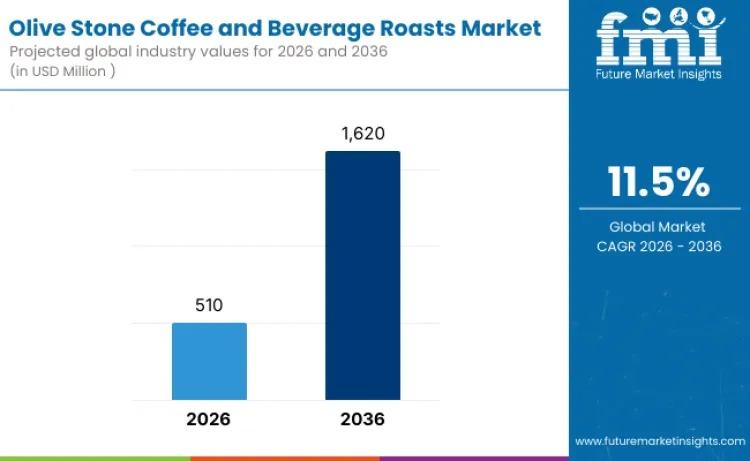
Global Olive Stone Coffee and Beverage Roasts Market to Reach USD 1,620 Million …
The global olive stone coffee and beverage roasts market is entering a high-growth decade, fueled by sustainability innovation and evolving specialty coffee culture. Valued at USD 510 million in 2026, the market is projected to reach USD 1,620 million by 2036, expanding at a compelling CAGR of 11.5%.
As consumers increasingly seek beverages that combine sustainability, functionality, and distinctive taste, olive stone-based roasting solutions are transitioning from niche experimentation to structured…
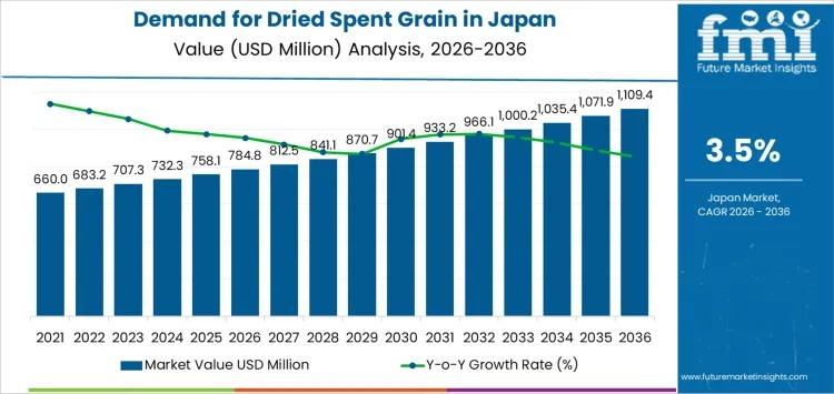
Japan Dried Spent Grain Market to Surpass USD 1.1 Billion by 2036 as Feed Optimi …
Japan's dried spent grain market is entering a decade of steady, value-driven expansion, supported by structured feed demand, brewery byproduct utilization, and rising integration of fiber-rich ingredients into food manufacturing. Industry estimates place the market at USD 784.8 million in 2026, with projections indicating growth to USD 1,109.4 million by 2036, reflecting a CAGR of 3.5%.
Between 2020 and 2026, demand increased from USD 637.5 million to USD 784.8 million, shaped…
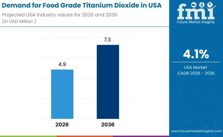
USA Food Grade Titanium Dioxide Market to Reach USD 7.3 Million by 2036 Amid Ste …
The demand for food grade titanium dioxide in the USA is valued at USD 4.9 million in 2026 and is projected to reach USD 7.3 million by 2036, expanding at a CAGR of 4.1%. Growth remains moderate yet stable, supported by continued use of titanium dioxide as a whitening and opacifying agent across confectionery coatings, bakery decorations, sauces, dairy analogues, and processed food matrices.
Despite heightened regulatory scrutiny and evolving clean-label…
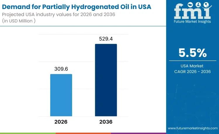
USA Partially Hydrogenated Oil Market to Reach USD 529.4 Million by 2036 Amid Me …
The demand for partially hydrogenated oil in the USA is projected to rise from USD 309.6 million in 2026 to USD 529.4 million by 2036, expanding at a steady CAGR of 5.5%. While edible applications remain tightly regulated, demand persists across specialty industrial and permitted food-related segments where oxidative stability, viscosity control, and texture performance remain critical.
Despite regulatory constraints on trans fats in conventional food manufacturing, PHOs continue to serve…
More Releases for Wafer
Semiconductor Silicon Wafer Market Is Going to Boom |• Silicon Wafer • Globa …
Worldwide Market Reports has released a new in-depth research study on the "Semiconductor Silicon Wafer Market," highlighting strong growth potential in the coming years. The report delivers a structured and data-driven analysis of the market landscape, combining robust research methodology, market sizing, validated data modeling, and insights sourced from reliable primary and secondary channels.
The study thoroughly examines key market aspects, including growth drivers, restraints, challenges, emerging opportunities, technological advancements, innovation…
Semiconductor Wafer Electrostatic Chucks for 300mm Wafer Market Size, Trends & F …
Semiconductor Wafer Electrostatic Chucks for 300mm Wafer Market Size
The global Semiconductor Wafer Electrostatic Chucks for 300mm Wafer market is projected to grow from US$ 1227 million in 2024 to US$ 1672.7 million by 2030, at a Compound Annual Growth Rate (CAGR) of 5.3% during the forecast period.
Get Free Sample: https://reports.valuates.com/request/sample/QYRE-Auto-38F13137/Global_Semiconductor_Wafer_Electrostatic_Chucks_for_300mm_Wafer_Market_Research_Report_2023?utm_source=openpr&utm_medium=referral
The US & Canada market for Semiconductor Wafer Electrostatic Chucks for 300mm Wafer is estimated to increase from $ million in…
Wafer Hybrid Bonding Equipment Market Share Driven by Wafer-to-Wafer Technology …
Wafer Hybrid Bonding Equipment Market Size
The global market for Wafer Hybrid Bonding Equipment was valued at US$ 164 million in the year 2024 and is projected to reach a revised size of US$ 756 million by 2031, growing at a CAGR of 24.7% during the forecast period.
View sample report
https://reports.valuates.com/request/sample/QYRE-Auto-31W14822/Global_Wafer_Hybrid_Bonding_Equipment_Market_Insights_Forecast_to_2029
The Wafer Hybrid Bonding Equipment market is experiencing accelerated growth, driven by increasing demand for advanced semiconductor packaging technologies that enable higher…
Semiconductor Wafer Electrostatic Chucks for 300mm Wafer Market
Semiconductor Wafer Electrostatic Chucks for 300mm Wafer Market
The global Semiconductor Wafer Electrostatic Chucks for 300mm Wafer market was valued at US$ 1165 million in 2023 and is anticipated to reach US$ 1672.7 million by 2030, witnessing a CAGR of 5.3% during the forecast period 2024-2030.
View Sample Report
https://reports.valuates.com/request/sample/QYRE-Auto-38F13137/Global_Semiconductor_Wafer_Electrostatic_Chucks_for_300mm_Wafer_Market_Research_Report_2023
Report Scope
The Semiconductor Wafer Electrostatic Chucks for 300mm Wafer market size, estimations, and forecasts are provided in terms of output/shipments (Units) and revenue…
Automatic Mounter Wafer Equipment Market Report 2018: Segmentation by Type (100 …
Global Automatic Mounter Wafer Equipment market research report provides company profile for Lintec Corporation, Nitto Denko, Tokyo Electron, Technovision, Takatori, Ultron Systems, DISCO Corp., Syagrus Systems, Advanced Dicing Technologies, Longhill Industries and Others.
This market study includes data about consumer perspective, comprehensive analysis, statistics, market share, company performances (Stocks), historical analysis 2012 to 2017, market forecast 2018 to 2025 in terms of volume, revenue, YOY growth rate, and CAGR for…
EMEA Solar Wafer Cutting Fluid PEG Market For Semiconductor, Solar Wafer, Crysta …
Latest industry research report on: EMEA (Europe, Middle East and Africa) Solar Wafer Cutting Fluid PEG Market : Industry Size, Share, Research, Reviews, Analysis, Strategies, Demand, Growth, Segmentation, Parameters, Forecasts
Request For Sample Report @ https://www.marketresearchreports.biz/sample/sample/1194694
Geographically, this report split EMEA into Europe, the Middle East and Africa, With sales (K MT), revenue (Million USD), market share and growth rate of Solar Wafer Cutting Fluid PEG for these regions, from 2012 to…
