Press release
Through Silicon Via (TSV) Packaging Market: Technological Development In IC Packaging

These are a high performance connection technique which are used as alternatives to flip chips and wire-bond to create 3D integrated circuits and 3D packages, paralleled to alternatives (package-on-package) as the compactness of the vias is considerably higher.
Moreover, the lengths of the connections are shorter. Technological development in IC packaging let the end product to be reduced in size such as tablets and smart phones. Silicon vias is a cutting-edge packaging technique where electronic goods occupies low space and offers superior connectivity. TSVs are used to unite several ICs organized in a single package.
The integration technology in semiconductors has been mostly present in two-dimensional applications in the recent past. These extensive applications have been employed not only in the area of the electronics but they are present in lot of associated businesses such as bioelectronics, military systems, submarine systems, computer systems, electronics analysis, medical systems, satellite systems optoelectronics, among others.
Request Brochure: https://www.transparencymarketresearch.com/sample/sample.php?flag=B&rep_id=21962
From the consumer’s point of view nearly all industrial products integrate semiconductor devices. One of the most significant reasons for this speedy growth is the better scalability of MOS or metal–oxide– semiconductor devices.
Based on type of platforms, the global through silicon via (TSV) packaging market can be bifurcated into 2.5D TSV platform and 3D TSV platform. 2.5D is primarily GPU (graphics processing unit) and CPU (central processing unit) driven whereas 3D is memory and application process driven. 2.5D TSV platform held a significant market share in the global through silicon via (TSV) packaging market.
This is due to the better functionalities and product opportunities available for 2,5D platforms such as it improves wafer yield, reduces wafer start cost, reduces complexity of manufacturing, improves power and performance. These factors will fuel the 2.5D TSV platform market thereby augmenting the overall growth of the global through silicon via (TSV) packaging market.
On the basis of application the through silicon via (TSV) packaging market can be classified into memory arrays, image sensors, graphics chips, MPUs (microprocessor units), DRAM (dynamic random access memory), integrated circuits, and others.
The complementary metal-oxide-semiconductor (CMOS) image sensor (CIS) was amongst the chief applications to implement TSV(s) in high volume engineering. In the initial phase of CIS applications, through silicon via were formed on the reverse of the wafer to form connects, eradicate wire links, thereby reducing form factor and higher-density links. These factors will drive the image sensors application segment in the overall through silicon via packaging market.
By geography, the global through silicon via (TSV) packaging market can be segmented into North America, Europe, Asia Pacific, Latin America, and the Middle East and Africa. Asia Pacific held the leading share of the market followed by North America.
Countries such as China, Korea and Japan utilizes silicon via (TSV) packaging on a large scale. These regions are considered as the hub of electronics parts manufacturing. Advancement in technology along with low cost manufacturing are the main reasons for growth in this region.
North America trailed Asia Pacific in terms of market share in the through silicon via (TSV) packaging market. Presence of large number of corporations along with kinship of consumers to adopt newer technology will drive the market in this region.
Some of the major players operating in the global exposure system market are Applied Materials, International Business Machines Corporation, Amkor Micralyne, Inc., Tezzaron Semiconductors, STATS ChipPAC Ltd, Micralyne, Inc., and Xilinx.
The report offers a comprehensive evaluation of the market. It does so via in-depth qualitative insights, historical data, and verifiable projections about market size. The projections featured in the report have been derived using proven research methodologies and assumptions.
By doing so, the research report serves as a repository of analysis and information for every facet of the market, including but not limited to: Regional markets, technology, types, and applications.
Book Now: https://www.transparencymarketresearch.com/through-silicon-via-packaging-market.html?secure=NTIxNS41&type=PB
About TMR
Transparency Market Research (TMR) is a global market intelligence company providing business information reports and services. The company’s exclusive blend of quantitative forecasting and trend analysis provides forward-looking insight for thousands of decision makers. TMR’s experienced team of analysts, researchers, and consultants use proprietary data sources and various tools and techniques to gather and analyze information.
TMR’s data repository is continuously updated and revised by a team of research experts so that it always reflects the latest trends and information. With extensive research and analysis capabilities, Transparency Market Research employs rigorous primary and secondary research techniques to develop distinctive data sets and research material for business reports.
Contact TMR
90 State Street, Suite 700
Albany, NY 12207
Tel: +1-518-618-1030
USA - Canada Toll Free: 866-552-3453
Email:sales@transparencymarketresearch.com
Website:http://www.transparencymarketresearch.com
This release was published on openPR.
Permanent link to this press release:
Copy
Please set a link in the press area of your homepage to this press release on openPR. openPR disclaims liability for any content contained in this release.
You can edit or delete your press release Through Silicon Via (TSV) Packaging Market: Technological Development In IC Packaging here
News-ID: 927005 • Views: …
More Releases from Transparency Market Research
Caustic Soda Market Size Forecast to USD 65.6 Billion by 2036 with Expanding App …
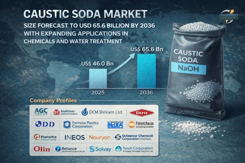
Caustic Soda Market Outlook 2036
The global caustic soda market was valued at US$ 46.0 Billion in 2025 and is projected to reach US$ 65.6 Billion by 2036, expanding at a steady CAGR of 3.2% from 2026 to 2036. Market growth is driven by increasing demand from the pulp & paper industry, rising alumina production, expanding chemical manufacturing activities, and growing applications in water treatment and textiles.
👉 Get your sample market…
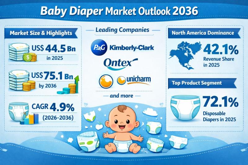
Global Baby Diaper Market Outlook 2036: Industry to Reach US$ 75.1 Billion by 20 …
The global baby diaper market was valued at US$ 44.5 Bn in 2025 and is projected to reach US$ 75.1 Bn by 2036, expanding at a steady CAGR of 4.9% from 2026 to 2036. This consistent upward trajectory reflects the essential nature of diapers in infant hygiene and the growing consumer preference for high-performance and convenient baby care products.
In 2025, North America accounted for 42.1% of the global revenue share,…
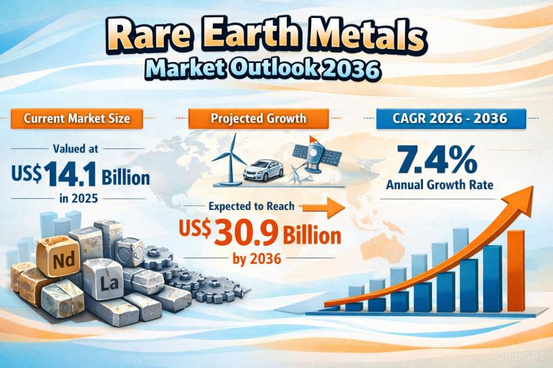
Rare Earth Metals Market to be Worth USD 30.9 Bn by 2036 - By Metal Type / By Ap …
The rare earth metals market has evolved from a niche industrial segment into a strategically critical global industry. In 2025, the market stood at US$ 14.1 Billion, driven primarily by increasing deployment of electric vehicles (EVs), renewable energy systems, defense electronics, and advanced industrial machinery.
Review critical insights and findings from our Report in this sample -
https://www.transparencymarketresearch.com/sample/sample.php?flag=S&rep_id=823
By 2036, the market is expected to nearly double to US$ 30.9 Billion, supported by…
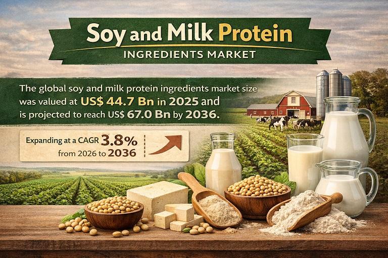
Soy and Milk Protein Ingredients Market to Reach USD 67.0 Billion by 2036 Amid R …
The global Soy and Milk Protein Ingredients Market is witnessing significant momentum as consumers increasingly prioritize high-protein diets, functional nutrition, and clean-label ingredients. With the surge in plant-based alternatives, sports nutrition products, and fortified food offerings, soy and milk protein ingredients have become critical components across multiple industries including food & beverages, pharmaceuticals, animal nutrition, and personal care.
The global Soy and Milk Protein Ingredients Market is projected to reach US$…
More Releases for TSV
TSV Electroplating Additive Market Size, Growth Opportunities and Forecast 2025- …
Los Angeles, United State: A newly published report titled "Global TSV Electroplating Additive Market Insights, Forecast to 2025-2031" by QY Research throws light on the industry dynamics and current and future trends that play a key role in determining the business expansion. The global TSV Electroplating Additive market was valued at US$ 224 million in 2024 and is anticipated to reach US$ 372 million by 2031, witnessing a CAGR of…
Through Silicon Via (TSV) Technology Market 2022 | Detailed Report
The Through Silicon Via (TSV) Technology report compiles the market information depending upon market development and growth factors, optimizing the growth path. In addition, it highlights the strategies and market share of the leading vendors in the particular market. The report follows a robust research methodology model that helps to make informed decisions. It obtains both qualitative and quantitative market information supported by primary research.
The Through Silicon Via (TSV) Technology…
Through Silicon Via (TSV) Technology Market 2021 | Detailed Report
Global Through Silicon Via (TSV) Technology Market 2021-2027, has been prepared based on an in-depth market analysis with inputs from industry experts. The report covers the market landscape and its growth prospects in the coming years. The report includes a discussion of the key vendors operating in this market. An exclusive data offered in this report is collected by research and industry experts team.
Get Free Sample PDF (including full TOC,…
3D TSV and 2.5D Market Size, Share, Development by 2024
Market Research Report Store offers a latest published report on 3D TSV and 2.5D Market Analysis and Forecast 2019-2025 delivering key insights and providing a competitive advantage to clients through a detailed report.
The global 3D TSV and 2.5D market is valued at xx million USD in 2018 and is expected to reach xx million USD by the end of 2024, growing at a CAGR of xx% between 2019 and 2024.
The…
Global 3D TSV Market Share and Growth 2019 - QY Research
3D TSV is a vertical electrical connection (via) that passes completely through a silicon wafer or die. TSVs are high performance interconnect techniques used as an alternative to wire-bond and flip chips to create 3D packages and 3D integrated circuits. Compared to alternatives such as package-on-package, the interconnect and device density is substantially higher, and the length of the connections becomes shorter.
The global 3D TSV market is valued at xx…
3D TSV Packages Market Value Chain and Forecast 2016-2026
Currently, 3D Packaging using Through Silicon Via technology (3D TSV) is one of the hottest topics in the semiconductor ecosystem. 3D TSV is vertical electrical connection (via) passing completely through a silicon wafer or die. These short vertical interconnects are replacing the long interconnects of 2D packaging technologies including wire-bond and flip chips.
Growing demand for high density and multifunctional microelectronics with improved performance, and the reduction of timing delays is…
