Press release
Global Wafer Level Package Dielectrics Market - Pin-Point Analysis For Changing Competitive Dynamics

Obtain Report Details @ http://www.transparencymarketresearch.com/wafer-level-package-dielectrics-market.html
The wafer level package dielectrics market is expected to expand at a healthy CAGR over the forecast period, and the major driving factor responsible for growth of the wafer level package dielectrics market is the rising demand for compact electronic devices with high performance and cost effective packaging in the semiconductor packaging industry. In case of conventional packaging, such as die level packaging, with the variation in size of the ICs, the cost of packaging becomes more as compared to the production cost of the ICs. On the contrary, wafer level packaging is much more cost-efficient as compared to the conventional packaging or the production cost of the ICs. The technological advancements in IC design & production are also, to an extent, propelling growth of the wafer level package dielectrics market currently. The wafer level packaging technology has certain perks over the traditional packaging technology, such as minimized electricity consumption and long battery life in case of mobile phones, and its compactness helps manufacturers design and develop ultra-thin mobile phones. However, fluctuations in some of the physical properties of the technology, such as the coefficient of thermal expansion of the materials of wafer with respect to the material of ICs, are considered as a drawback of the wafer packaging technology, which in turn might restraint growth of the market for wafer level package dielectrics.
The global wafer level package dielectrics market is segmented on the basis of type of wafer level packaging, application, and region. On the basis of type, the global market for wafer level package dielectrics is segmented into FOWLP (Fan-Out Wafer Level Package), FIWLP (Fan-in Wafer Level Package), FIWLCSP (Fan-in Wafer Level Chip Scale Package), flip chip, and 3DFOWLP. On the basis of applications, the global market for wafer level package is segmented into consumer electronics, automotive, aerospace, defense, and healthcare.
Fill the form to gain deeper insights on this market @ http://www.transparencymarketresearch.com/sample/sample.php?flag=B&rep_id=9551
On the basis of geography, the global rigid plastic packaging market is segmented into seven key regions, namely North America, Latin America, Western Europe, Eastern Europe, Asia Pacific, Japan, and the Middle East & Africa. Among the aforementioned regions, the Asia-Pacific market is projected to grow at a promising CAGR, which is attributed to the increase in demand for smart phones globally. For instance, recently, India become the second largest user of smart phones globally, beating the U.S. This is turn is expected to drive growth of the wafer level package dielectrics market in the country. Moreover, the presence of leading semiconductor manufacturers, such as Taiwan Semiconductor Manufacturing, among others, is expected to have a positive effect on growth of the wafer level package dielectrics market in APEJ over the forecast period.
Some of the major players identified in the global wafer level package dielectrics market include ChipMOS TECHNOLOGIES INC., STATS ChipPAC Ltd., IQE PLC, Amkor Technology Inc., TriQuint Semiconductor Inc., Deca Technologies, KLA-Tencor Corporation, Siliconware Precision Industries Co. Ltd., China Wafer Level CSP Co. Ltd., and Jiangsu Changjiang Electronics Technology Co. Ltd.
About TMR
TMR is a global market intelligence company providing business information reports and services. The company’s exclusive blend of quantitative forecasting and trend analysis provides forward-looking insight for thousands of decision makers. TMR’s experienced team of analysts, researchers, and consultants use proprietary data sources and various tools and techniques to gather and analyze information.
Contact TMR
90 State Street, Suite 700
Albany, NY 12207
Tel: +1-518-618-1030
USA - Canada Toll Free: 866-552-3453
Email: sales@transparencymarketresearch.com
Website: http://www.transparencymarketresearch.com
This release was published on openPR.
Permanent link to this press release:
Copy
Please set a link in the press area of your homepage to this press release on openPR. openPR disclaims liability for any content contained in this release.
You can edit or delete your press release Global Wafer Level Package Dielectrics Market - Pin-Point Analysis For Changing Competitive Dynamics here
News-ID: 613142 • Views: …
More Releases from Transparency Market Research
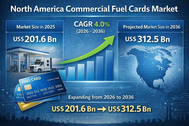
North America Commercial Fuel Cards Market Growth Accelerates Toward USD 312.5 B …
The North America commercial fuel cards market is expanding steadily as businesses seek greater control over fuel expenses, fleet efficiency, and operational transparency. Commercial fuel cards are payment tools designed specifically for businesses that operate vehicle fleets, enabling them to monitor fuel usage, manage expenses, reduce fraud, and simplify accounting processes. These cards are widely used across transportation, logistics, construction, utilities, and service industries.
The North America Commercial Fuel Cards Market…
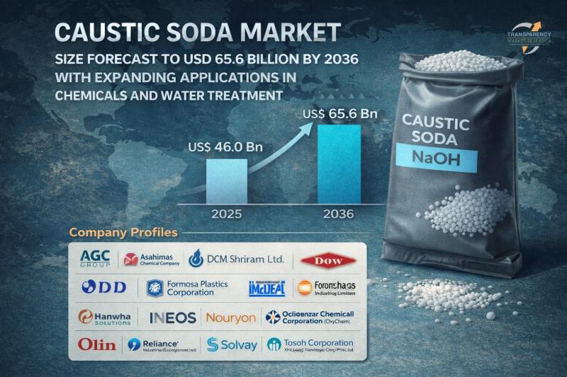
Caustic Soda Market Size Forecast to USD 65.6 Billion by 2036 with Expanding App …
Caustic Soda Market Outlook 2036
The global caustic soda market was valued at US$ 46.0 Billion in 2025 and is projected to reach US$ 65.6 Billion by 2036, expanding at a steady CAGR of 3.2% from 2026 to 2036. Market growth is driven by increasing demand from the pulp & paper industry, rising alumina production, expanding chemical manufacturing activities, and growing applications in water treatment and textiles.
👉 Get your sample market…
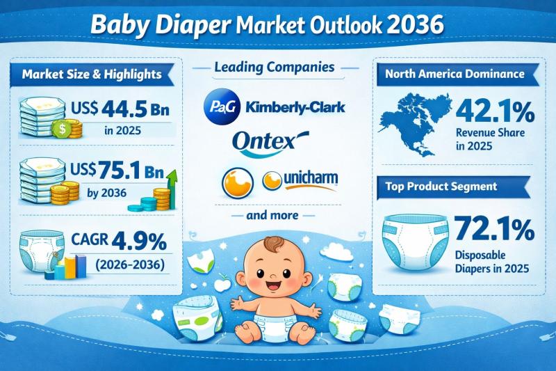
Global Baby Diaper Market Outlook 2036: Industry to Reach US$ 75.1 Billion by 20 …
The global baby diaper market was valued at US$ 44.5 Bn in 2025 and is projected to reach US$ 75.1 Bn by 2036, expanding at a steady CAGR of 4.9% from 2026 to 2036. This consistent upward trajectory reflects the essential nature of diapers in infant hygiene and the growing consumer preference for high-performance and convenient baby care products.
In 2025, North America accounted for 42.1% of the global revenue share,…
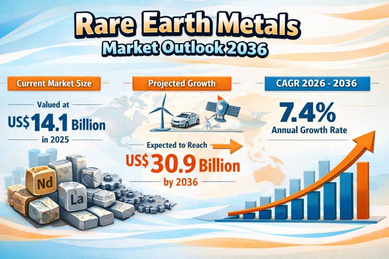
Rare Earth Metals Market to be Worth USD 30.9 Bn by 2036 - By Metal Type / By Ap …
The rare earth metals market has evolved from a niche industrial segment into a strategically critical global industry. In 2025, the market stood at US$ 14.1 Billion, driven primarily by increasing deployment of electric vehicles (EVs), renewable energy systems, defense electronics, and advanced industrial machinery.
Review critical insights and findings from our Report in this sample -
https://www.transparencymarketresearch.com/sample/sample.php?flag=S&rep_id=823
By 2036, the market is expected to nearly double to US$ 30.9 Billion, supported by…
More Releases for Wafer
Semiconductor Silicon Wafer Market Is Going to Boom |• Silicon Wafer • Globa …
Worldwide Market Reports has released a new in-depth research study on the "Semiconductor Silicon Wafer Market," highlighting strong growth potential in the coming years. The report delivers a structured and data-driven analysis of the market landscape, combining robust research methodology, market sizing, validated data modeling, and insights sourced from reliable primary and secondary channels.
The study thoroughly examines key market aspects, including growth drivers, restraints, challenges, emerging opportunities, technological advancements, innovation…
Semiconductor Wafer Electrostatic Chucks for 300mm Wafer Market Size, Trends & F …
Semiconductor Wafer Electrostatic Chucks for 300mm Wafer Market Size
The global Semiconductor Wafer Electrostatic Chucks for 300mm Wafer market is projected to grow from US$ 1227 million in 2024 to US$ 1672.7 million by 2030, at a Compound Annual Growth Rate (CAGR) of 5.3% during the forecast period.
Get Free Sample: https://reports.valuates.com/request/sample/QYRE-Auto-38F13137/Global_Semiconductor_Wafer_Electrostatic_Chucks_for_300mm_Wafer_Market_Research_Report_2023?utm_source=openpr&utm_medium=referral
The US & Canada market for Semiconductor Wafer Electrostatic Chucks for 300mm Wafer is estimated to increase from $ million in…
Wafer Hybrid Bonding Equipment Market Share Driven by Wafer-to-Wafer Technology …
Wafer Hybrid Bonding Equipment Market Size
The global market for Wafer Hybrid Bonding Equipment was valued at US$ 164 million in the year 2024 and is projected to reach a revised size of US$ 756 million by 2031, growing at a CAGR of 24.7% during the forecast period.
View sample report
https://reports.valuates.com/request/sample/QYRE-Auto-31W14822/Global_Wafer_Hybrid_Bonding_Equipment_Market_Insights_Forecast_to_2029
The Wafer Hybrid Bonding Equipment market is experiencing accelerated growth, driven by increasing demand for advanced semiconductor packaging technologies that enable higher…
Semiconductor Wafer Electrostatic Chucks for 300mm Wafer Market
Semiconductor Wafer Electrostatic Chucks for 300mm Wafer Market
The global Semiconductor Wafer Electrostatic Chucks for 300mm Wafer market was valued at US$ 1165 million in 2023 and is anticipated to reach US$ 1672.7 million by 2030, witnessing a CAGR of 5.3% during the forecast period 2024-2030.
View Sample Report
https://reports.valuates.com/request/sample/QYRE-Auto-38F13137/Global_Semiconductor_Wafer_Electrostatic_Chucks_for_300mm_Wafer_Market_Research_Report_2023
Report Scope
The Semiconductor Wafer Electrostatic Chucks for 300mm Wafer market size, estimations, and forecasts are provided in terms of output/shipments (Units) and revenue…
Automatic Mounter Wafer Equipment Market Report 2018: Segmentation by Type (100 …
Global Automatic Mounter Wafer Equipment market research report provides company profile for Lintec Corporation, Nitto Denko, Tokyo Electron, Technovision, Takatori, Ultron Systems, DISCO Corp., Syagrus Systems, Advanced Dicing Technologies, Longhill Industries and Others.
This market study includes data about consumer perspective, comprehensive analysis, statistics, market share, company performances (Stocks), historical analysis 2012 to 2017, market forecast 2018 to 2025 in terms of volume, revenue, YOY growth rate, and CAGR for…
EMEA Solar Wafer Cutting Fluid PEG Market For Semiconductor, Solar Wafer, Crysta …
Latest industry research report on: EMEA (Europe, Middle East and Africa) Solar Wafer Cutting Fluid PEG Market : Industry Size, Share, Research, Reviews, Analysis, Strategies, Demand, Growth, Segmentation, Parameters, Forecasts
Request For Sample Report @ https://www.marketresearchreports.biz/sample/sample/1194694
Geographically, this report split EMEA into Europe, the Middle East and Africa, With sales (K MT), revenue (Million USD), market share and growth rate of Solar Wafer Cutting Fluid PEG for these regions, from 2012 to…
