Press release
3D TSV Packages Market Analysis and Value Forecast Snapshot by End-use Industry 2016-2026

Growing demand for high density and multifunctional microelectronics with improved performance, and the reduction of timing delays is currently driving the market for 3D TSV packages. . However, the challenges encountered during assembly and packaging, handling ultrathin semiconductor components in front-end and back-end process owing to its fragility are some of the factors restraining the market growth.
Market Overview:
Several 3D packages, such as System in Package and Chip Stack MCM, are available in the market providing smaller form factor and greater connectivity. The stacked chips are wired together along their edges in these packages. This wiring increases the length and width of the package, thus requiring an extra “interposer” layer between the chips. The new 3D TSV package creates vertical connections through the body of the chips, replacing edge wiring and in turn reducing the extra added length and width.
Request Report Sample@ http://www.futuremarketinsights.com/reports/sample/rep-gb-1398
3D TSV technology allows stacking of LSIs which facilitates manufacturing of smaller products such as wearable devices. , Semiconductor fabricators globally are adopting 3D TSV technology in order to cater to the increasing requirements of functional integration.
Market Dynamics:
Growing demand for innovative chip architectures with improved features such as low power consumption, high aspect ratio, and smaller form factor is driving the market of 3D TSV packages. Additionally, factors such as proliferation in the cloud based applications, robust outlook for the Information & Communication Technologies segment, and persistent developments in the DRAM and smart lighting sectors are further cementing the adoption of 3D TSV packages for fabrication process.
The market is expected to witness potential revenue opportunity mainly due to growth in its application areas such as MEMS, CMOS image sensors, optoelectronics and high end LED solutions. Additionally, 3D TSV packages are expected to gain more traction in its adoption in the DRAM memory domain with the advent of innovative technologies such as HMC (Hybrid Memory Cube) and HBM (High Bandwidth Memory).
Several challenges are encountered while handling this wafer for packaging process as the TSV wafer is thinned down to the thickness of 40-50um. TSV wafers are thinned in order to meet the diverse needs, including temporary adhesion strength, and chemical and thermal stability in the fabrication process. These challenges are constraining the growth of the market and are expected to continue hampering the market growth during the forecast period. Furthermore, 3D TSV assembly process is more complex, compared to traditional flip-chip process which is also one of the primary constraint for this market.
With the up surging demand for improved and advanced electronic products having smaller form factor, superior functionality, reduced power consumption with a lower overall cost the market is expected to witness adoption of advanced packaging technologies such as 3D TSV during the forecast period.
Market Segmentation:
3D TSV Packages market is mainly classified on the basis of process realization, applications, verticals and geography.
On the basis of process realization, 3D TSV Packages market is segmented as:
via first
via middle
via last segments
On the basis of applications, 3D TSV Packages is segmented as:
Logic & memory devices
MEMS & sensors
Power & analog components
The basis of verticals, 3D TSV Packages is segmented as:
Consumer electronics
Information & Communication Technologies
Automotive
Military & defense
Other sectors (aerospace and medical)
On the basis of geography, global market of 3D TSV Devices is segmented as:
North America
Latin America
Western Europe
Eastern Europe
Asia Pacific Excluding Japan
Japan
Middle East & Africa
Visit For TOC@ http://www.futuremarketinsights.com/toc/rep-gb-1398
Key Market Players
The leading players of this industry include Amkor Technology Inc., Jiangsu Changjiang Electronics Technology Co. (STATS chipPAC), Toshiba Electronics Co.Ltd., Samsung Electronics Co.Ltd., Taiwan Semiconductor Manufacturing Company Limited (TSMC), United Microelectronics Corporation, Xilinx Inc., Teledyne DALSA Inc., and Tezzaron Semiconductor Corporation.
About Us – Future Market Insights is the premier provider of market intelligence and consulting services, serving clients in over 150 countries. FMI is headquartered in London, the global financial capital, and has delivery centers in the U.S. and India.
CONTACT:
616 Corporate Way, Suite 2-9018,
Valley Cottage, NY 10989,
United States
T: +1-347-918-3531
F: +1-845-579-5705
Email: sales@futuremarketinsights.com
Website: www.futuremarketinsights.com
This release was published on openPR.
Permanent link to this press release:
Copy
Please set a link in the press area of your homepage to this press release on openPR. openPR disclaims liability for any content contained in this release.
You can edit or delete your press release 3D TSV Packages Market Analysis and Value Forecast Snapshot by End-use Industry 2016-2026 here
News-ID: 584925 • Views: …
More Releases from Future Market Insights
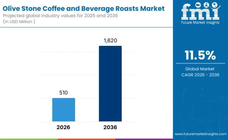
Global Olive Stone Coffee and Beverage Roasts Market to Reach USD 1,620 Million …
The global olive stone coffee and beverage roasts market is entering a high-growth decade, fueled by sustainability innovation and evolving specialty coffee culture. Valued at USD 510 million in 2026, the market is projected to reach USD 1,620 million by 2036, expanding at a compelling CAGR of 11.5%.
As consumers increasingly seek beverages that combine sustainability, functionality, and distinctive taste, olive stone-based roasting solutions are transitioning from niche experimentation to structured…
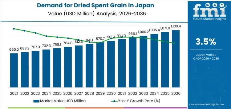
Japan Dried Spent Grain Market to Surpass USD 1.1 Billion by 2036 as Feed Optimi …
Japan's dried spent grain market is entering a decade of steady, value-driven expansion, supported by structured feed demand, brewery byproduct utilization, and rising integration of fiber-rich ingredients into food manufacturing. Industry estimates place the market at USD 784.8 million in 2026, with projections indicating growth to USD 1,109.4 million by 2036, reflecting a CAGR of 3.5%.
Between 2020 and 2026, demand increased from USD 637.5 million to USD 784.8 million, shaped…
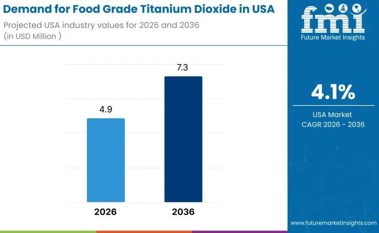
USA Food Grade Titanium Dioxide Market to Reach USD 7.3 Million by 2036 Amid Ste …
The demand for food grade titanium dioxide in the USA is valued at USD 4.9 million in 2026 and is projected to reach USD 7.3 million by 2036, expanding at a CAGR of 4.1%. Growth remains moderate yet stable, supported by continued use of titanium dioxide as a whitening and opacifying agent across confectionery coatings, bakery decorations, sauces, dairy analogues, and processed food matrices.
Despite heightened regulatory scrutiny and evolving clean-label…
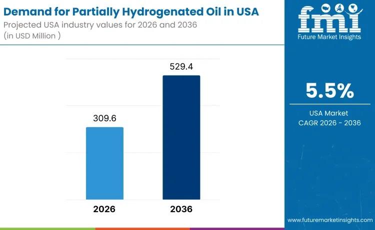
USA Partially Hydrogenated Oil Market to Reach USD 529.4 Million by 2036 Amid Me …
The demand for partially hydrogenated oil in the USA is projected to rise from USD 309.6 million in 2026 to USD 529.4 million by 2036, expanding at a steady CAGR of 5.5%. While edible applications remain tightly regulated, demand persists across specialty industrial and permitted food-related segments where oxidative stability, viscosity control, and texture performance remain critical.
Despite regulatory constraints on trans fats in conventional food manufacturing, PHOs continue to serve…
More Releases for TSV
TSV Electroplating Additive Market Size, Growth Opportunities and Forecast 2025- …
Los Angeles, United State: A newly published report titled "Global TSV Electroplating Additive Market Insights, Forecast to 2025-2031" by QY Research throws light on the industry dynamics and current and future trends that play a key role in determining the business expansion. The global TSV Electroplating Additive market was valued at US$ 224 million in 2024 and is anticipated to reach US$ 372 million by 2031, witnessing a CAGR of…
Through Silicon Via (TSV) Technology Market 2022 | Detailed Report
The Through Silicon Via (TSV) Technology report compiles the market information depending upon market development and growth factors, optimizing the growth path. In addition, it highlights the strategies and market share of the leading vendors in the particular market. The report follows a robust research methodology model that helps to make informed decisions. It obtains both qualitative and quantitative market information supported by primary research.
The Through Silicon Via (TSV) Technology…
Through Silicon Via (TSV) Technology Market 2021 | Detailed Report
Global Through Silicon Via (TSV) Technology Market 2021-2027, has been prepared based on an in-depth market analysis with inputs from industry experts. The report covers the market landscape and its growth prospects in the coming years. The report includes a discussion of the key vendors operating in this market. An exclusive data offered in this report is collected by research and industry experts team.
Get Free Sample PDF (including full TOC,…
3D TSV and 2.5D Market Size, Share, Development by 2024
Market Research Report Store offers a latest published report on 3D TSV and 2.5D Market Analysis and Forecast 2019-2025 delivering key insights and providing a competitive advantage to clients through a detailed report.
The global 3D TSV and 2.5D market is valued at xx million USD in 2018 and is expected to reach xx million USD by the end of 2024, growing at a CAGR of xx% between 2019 and 2024.
The…
Global 3D TSV Market Share and Growth 2019 - QY Research
3D TSV is a vertical electrical connection (via) that passes completely through a silicon wafer or die. TSVs are high performance interconnect techniques used as an alternative to wire-bond and flip chips to create 3D packages and 3D integrated circuits. Compared to alternatives such as package-on-package, the interconnect and device density is substantially higher, and the length of the connections becomes shorter.
The global 3D TSV market is valued at xx…
3D TSV Packages Market Value Chain and Forecast 2016-2026
Currently, 3D Packaging using Through Silicon Via technology (3D TSV) is one of the hottest topics in the semiconductor ecosystem. 3D TSV is vertical electrical connection (via) passing completely through a silicon wafer or die. These short vertical interconnects are replacing the long interconnects of 2D packaging technologies including wire-bond and flip chips.
Growing demand for high density and multifunctional microelectronics with improved performance, and the reduction of timing delays is…
