


Press release
$100 Billion U.S. Semiconductor Expansion Accelerates the Shift Toward Localized Advanced Packaging
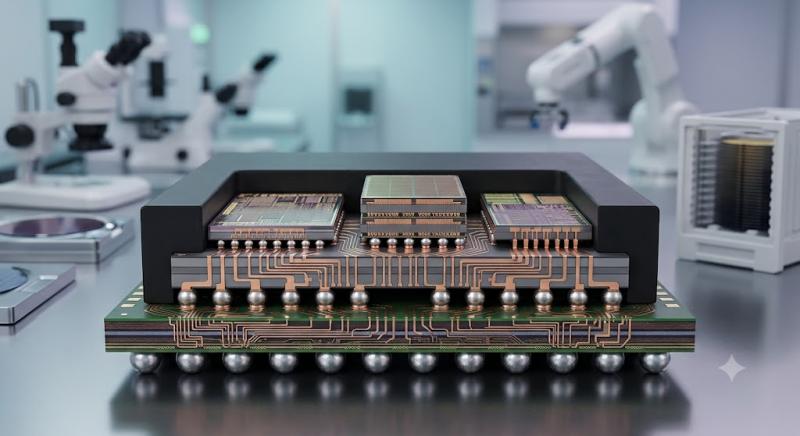
Advanced Packaging Semiconductor Market
The headline $100 billion expansion announced for U.S. semiconductor manufacturing includes plans for advanced packaging infrastructure, making packaging localization a strategic supply chain priority rather than a downstream manufacturing decision. This shift is changing procurement toward integrated foundry, packaging, and testing capabilities, while increasing demand for 2.5D and 3D integration, through silicon vias (TSVs), hybrid bonding, redistribution layers, and advanced interconnects. Traditional packaging approaches face pressure where performance, thermal management, and integration density become critical.
According to DataM Intelligence, the global Advanced Packaging Semiconductor Market reached US 22.48billion in 2025 and is projected to reach US 46.98 billion by 2035, growing at a 7.8% CAGR during 2026-2035. Asia-Pacific remains a major manufacturing and packaging hub, supported by concentrated semiconductor production and advanced packaging infrastructure, while North America is gaining strategic importance through AI infrastructure and supply-chain localization. Demand is particularly tied to data centers and AI, with 2.5D and 3D packaging, chiplet architectures, HBM integration, TSVs, and hybrid bonding becoming increasingly important to next-generation processors and memory systems.
Request Exclusive Sample (Top Performing Strategies - Next 5 Years):
https://www.datamintelligence.com/download-sample/advanced-packaging-semiconductor-market?praneetha
The commercial opportunity is shifting toward suppliers that can combine high density packaging, thermal management, advanced interconnects, and high volume manufacturing. TSMC, Samsung Electronics, Intel, ASE Technology, Amkor Technology, and JCET are positioned across different parts of the advanced packaging ecosystem. AI accelerators and HBM are particularly important because they require tighter integration between logic and memory. Customers are increasingly evaluating packaging capability alongside wafer fabrication, creating opportunities for integrated manufacturing models, localized capacity, and application specific packaging services.
The competitive landscape is also being reshaped by large-scale localization investments. In 2025, TSMC announced an additional $100 billion investment in the United States, taking its planned U.S. investment to $165 billion and including three additional fabrication facilities, two advanced packaging facilities, and an R&D center. The move strengthens the U.S. advanced semiconductor supply chain and gives customers a path toward domestically produced chips combined with advanced packaging. It also increases competitive pressure on OSAT providers and other packaging suppliers to expand capacity near major foundry and AI-chip ecosystems.
Regional dynamics increasingly reflect the localization of strategically important semiconductor capabilities. Asia-Pacific maintains a strong position because Taiwan, South Korea, China, Japan, and Southeast Asia host extensive semiconductor manufacturing, assembly, testing, and materials ecosystems. North America is becoming a major investment destination as government incentives and private capital support domestic semiconductor production and advanced packaging. The United States is particularly important for AI and high performance computing supply chains, while South Korea continues to strengthen its role in memory and HBM related packaging infrastructure.
The market's technology transition is centered on 2.5D and 3D integration, where multiple dies or memory components are assembled into high performance systems. 2.5D packaging is closely linked with AI accelerators and HBM because it enables high bandwidth connections between processors and memory. At the interconnect level, TSVs, hybrid bonding, copper pillars, and advanced RDL technologies are gaining relevance as conventional scaling becomes less sufficient for performance improvements. The result is a shift from package level optimization toward co-design of chip, interconnect, thermal architecture, and package.
Recent Developments
March 2026 - TSMC: TSMC expanded its U.S. advanced semiconductor manufacturing plans to support growing demand for AI infrastructure, with its broader U.S. investment program reaching approximately $165 billion. The expansion includes additional advanced fabrication and packaging capabilities, reinforcing the shift toward localized production of high performance AI chips and advanced semiconductor packages.
April 2025 - TSMC: TSMC announced an additional $100 billion investment in U.S. semiconductor manufacturing, bringing its planned U.S. investment to $165 billion. The expansion includes three additional fabs, two advanced packaging facilities, and an R&D center, directly strengthening localized advanced packaging capacity.
February 2025 - SK hynix: SK hynix advanced its U.S. semiconductor strategy around its planned Indiana facility, which includes an advanced packaging and R&D operation focused on next-generation memory products. The project supports the localization of HBM-related manufacturing and packaging capabilities for AI infrastructure.
Purchase This Exclusive Report:
https://www.datamintelligence.com/buy-now-page?report=advanced-packaging-semiconductor-market?praneetha
Additional Benefits:
✅ Get Interactive Dashboard Access (With No Additional Cost)
✅ Three months of analyst support to answer queries related to the report.
Company Profiles
TSMC: TSMC provides advanced packaging technologies including CoWoS, InFO, and SoIC for high performance computing, AI, and mobile applications. Its 2025 U.S. expansion includes two planned advanced packaging facilities, strengthening its ability to combine wafer fabrication and packaging within a localized ecosystem. This integrated model is increasingly important as AI customers require coordinated wafer, HBM, interconnect, and packaging capacity.
Samsung Electronics: Samsung combines foundry, memory, and advanced packaging capabilities, giving it a vertically integrated position across logic and memory applications. Its advanced packaging portfolio supports heterogeneous integration and high performance computing requirements. The company's combination of HBM, foundry, and packaging capabilities is strategically relevant as customers seek tighter integration between processors and high bandwidth memory.
Intel: Intel's advanced packaging portfolio includes technologies such as EMIB and Foveros, supporting chiplet-based and 3D architectures. Its U.S. manufacturing footprint and Arizona investment in additional advanced packaging capacity support domestic supply chain development. Intel's technology position is particularly relevant to customers adopting heterogeneous architectures that require high density die-to-die integration.
ASE Technology: ASE provides advanced semiconductor assembly and test services and has expanded capabilities around heterogeneous integration, fan out, wafer level packaging, and other advanced packaging technologies. Its OSAT model gives chip companies access to packaging capacity without requiring complete internal packaging infrastructure, making it relevant as demand expands across AI, automotive, communications, and high performance computing.
Amkor Technology: Amkor provides advanced packaging and testing services across applications including AI, communications, automotive, and consumer electronics. Its planned Arizona facility is strategically important because it expands advanced packaging and test capabilities in the United States. The company's role illustrates the increasing importance of geographically distributed OSAT capacity alongside localized wafer manufacturing.
JCET: JCET operates across semiconductor assembly and testing, including advanced packaging technologies serving automotive, communications, computing, and consumer applications. Its portfolio supports the transition toward higher-density packaging and heterogeneous integration. As customers diversify manufacturing footprints, large OSAT providers with established Asian production infrastructure can remain important partners for scalable advanced packaging deployment.
Other notable market participants include ASE Technology Holding Co., Amkor Technology, JCET Group, Powertech Technology, and ChipMOS Technologies.
Ready to Expand in the Market? Find the Right Partners Today:
https://www.datamintelligence.com/partner-identification-enquiry/advanced-packaging-semiconductor-market?praneetha
The Advanced Packaging Semiconductor Market is shifting from conventional package assembly toward tightly integrated chip, memory, interconnect, and thermal architectures. Customers are increasingly buying packaging as a performance enabling component of the semiconductor system rather than treating it as a final manufacturing step. AI accelerators, HBM, chiplets, 2.5D integration, and 3D stacking are therefore changing both technology selection and supplier requirements.
Asia-Pacific retains the strongest manufacturing ecosystem, while North America is becoming more important as semiconductor localization moves advanced packaging into strategic investment plans. The most attractive opportunities are concentrated around AI and high performance computing, HBM integration, 2.5D and 3D packaging, hybrid bonding, and advanced interconnects. Competitive advantage will increasingly depend on packaging capacity, technology integration, supply reliability, geographic localization, and the ability to support customers from wafer fabrication through advanced assembly and testing.
For More Information:
https://www.datamintelligence.com/research-report/advanced-packaging-semiconductor-market
Request for 2 Days FREE Dashboard Access:
https://www.datamintelligence.com/reports-subscription
☛ Power your decisions with real-time competitor tracking, strategic forecasts and global investment insights all in one place.
✅ Competitive Landscape
✅ Sustainability Impact Analysis
✅ KOL / Stakeholder Insights
✅ Unmet Needs & Positioning, Pricing & Market Access Snapshots
✅ Market Volatility & Emerging Risks Analysis
✅ Quarterly Industry Report Updated
✅ Live Market & Pricing Trends
✅ Import-Export Data Monitoring
Contact Us:
Sai Kiran
Business Development Manager
DataM Intelligence 4market Research LLP
6th Floor, M2 Tech Hub, Lalitha Nagar, Habsiguda,
Secunderabad, Hyderabad, Telangana 500039
USA: +1 877-441-4866
Email: Sai.k@datamintelligence.com
About DataM Intelligence
DataM Intelligence is a market research and consulting firm delivering end-to-end business intelligence solutions across syndicated research, customized studies, competitive intelligence and strategic consulting. The company helps organizations identify growth opportunities, understand competitive developments and support informed business decisions across more than 50 countries worldwide.
This release was published on openPR.
Permanent link to this press release:
Copy
Please set a link in the press area of your homepage to this press release on openPR. openPR disclaims liability for any content contained in this release.
You can edit or delete your press release $100 Billion U.S. Semiconductor Expansion Accelerates the Shift Toward Localized Advanced Packaging here
News-ID: 4663553 • Views: …
More Releases from DataM Intelligence 4Market Research LLP
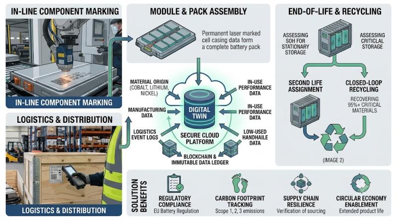
Battery Traceability Solutions Market (2035): Digital Battery Passports, Circulo …
The Battery Traceability Solutions Market was valued at US$546 million in 2025 and is projected to reach US$1,034.5 million by 2035, growing at a CAGR of 6.6% during 2026-2035.
DataM Intelligence has released its latest "Battery Traceability Solutions Market Size 2026" report, offering insights into market trends, emerging technologies, competitive developments, and regional opportunities. The report examines market size, growth forecasts, deployment models, and key applications, including electric vehicles, battery energy…
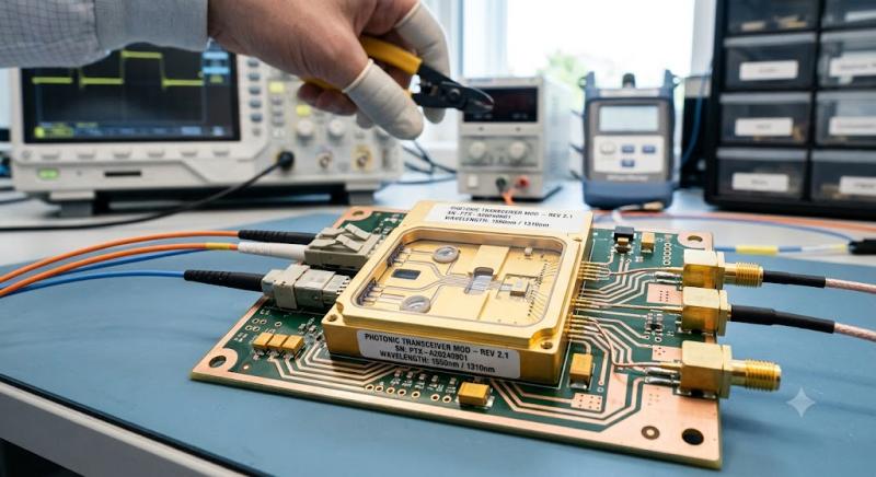
Photonic Packaging Market (2035): AI Data Centers, Co-Packaged Optics, Silicon P …
The Photonics Packaging Market was valued at US$ 2.96 billion in 2025 and is projected to reach US$ 6.19 billion by 2035, growing at a CAGR of 7.65% during 2026-2035.
DataM Intelligence has released its latest "Photonics Packaging Market Size 2026" report, offering detailed insights into market trends, technology developments, competitive dynamics, and regional opportunities. The report examines market size, growth forecasts, packaging technologies, key components, and emerging applications across data…
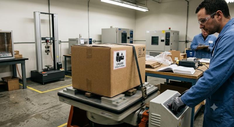
Battery Packaging Market (2035): CATL, Amcor, Nefab, EV Battery Safety, Sustaina …
The Battery Packaging Market is valued at US$39.5 billion in 2025 and is projected to reach US$116.45 billion by 2035, growing at a CAGR of 11.6% during 2026-2035.DataM Intelligence has released its latest "Battery Packaging Market Size 2026" report, offering insights into market trends, competitive developments, regional performance, and emerging business opportunities. The report examines market size by value and volume, CAGR forecasts, packaging technologies, material innovations, and developments across…

Pharmaceutical Microbiology QC Testing Market (2033): Rapid Sterility Testing, F …
The global pharmaceutical microbiology QC testing market was valued at US$4.05 billion in 2025 and is projected to reach US$10.84 billion by 2033, growing at a compound annual growth rate (CAGR) of 13.1% during 2026-2033.
DataM Intelligence has released its latest "Pharmaceutical Microbiology QC Testing Market Size 2026" report, providing insights into market trends, regulatory developments, testing technologies, competitive dynamics, and regional opportunities. The report examines market size by value, growth…
More Releases for HBM
DRAM Market Dynamics: Navigating HBM Wafer Shortages & Pricing Volatility
DRAM Market size was valued at US$ 126 Bn. in 2025 and the total DRAM Market revenue is expected to grow at 6 % from 2026 to 2032, reaching nearly US$ 189.46 Bn.
DRAM Market Overview:
The Dynamic Random-Access Memory (DRAM) market is navigating a monumental structural shift, moving rapidly from a traditional cyclical commodity toward an AI-driven, high-value specialty market. Valued at US$ 126 Billion in 2025, the total DRAM industry…
Global HBM Storage Tester Market Analysis (2025-2031)
LPI (LP Information)' newest research report, the "HBM Storage Tester Industry Forecast" looks at past sales and reviews total world HBM Storage Tester sales in 2025, providing a comprehensive analysis by region and market sector of projected HBM Storage Tester sales for 2025 through 2031. With HBM Storage Tester sales broken down by region, market sector and sub-sector, this report provides a detailed analysis in US$ millions of the world…
High Bandwidth Memory (HBM) Market Size Analysis by Application, Type, and Regio …
USA, New Jersey- According to Market Research Intellect, the global High Bandwidth Memory (HBM) market in the Internet, Communication and Technology category is projected to witness significant growth from 2025 to 2032. Market dynamics, technological advancements, and evolving consumer demand are expected to drive expansion during this period.
Because High Bandwidth Memory (HBM) is essential for improving data transmission speeds for high-performance computer applications, the market for HBM is expanding significantly.…
HBM Chips for AI Servers Market
HBM Chips for AI Servers Market Overview
High-Bandwidth Memory (HBM) chips are advanced types of memory designed to offer significantly higher bandwidth compared to traditional DRAM (Dynamic Random-Access Memory) technologies. Developed collaboratively by AMD and Hynix and now standardized by JEDEC, HBM chips are particularly important in applications requiring large amounts of data to be transferred quickly, such as graphics processing units (GPUs), high-performance computing (HPC), artificial intelligence (AI), and data…
High Bandwidth Memory (HBM) for AI Chipsets Market
High Bandwidth Memory (HBM) for AI Chipsets Market Overview
High-Bandwidth Memory (HBM) chips are advanced types of memory designed to offer significantly higher bandwidth compared to traditional DRAM (Dynamic Random-Access Memory) technologies. Developed collaboratively by AMD and Hynix and now standardized by JEDEC, HBM chips are particularly important in applications requiring large amounts of data to be transferred quickly, such as graphics processing units (GPUs), high-performance computing (HPC), artificial intelligence (AI),…
Global Strain Gauges Market 2018 - VPG, HBM, Zemic, Yiling
Apex Market Reports, recently published a detailed market research study focused on the "Strain Gauges Market" across the global, regional and country level. The report provides 360° analysis of "Strain Gauges Market" from view of manufacturers, regions, product types and end industries. The research report analyses and provides the historical data along with current performance of the global Strain Gauges industry, and estimates the future trend of Strain Gauges market…

