


Press release
Global Semiconductor High-End Bonding Equipment Market to Reach US$6.48 Billion by 2032, LP Information Finds

Semiconductor high-end bonding equipment refers to core process equipment used to create high-precision, ultra-clean and highly reliable bonding interfaces between wafer-to-wafer (W2W), die-to-wafer / chip-to-wafer (D2W/C2W), or chip-to-chip (C2C) structures for advanced packaging, heterogeneous integration, Chiplet, HBM, CIS, MEMS, silicon photonics / CPO and advanced logic 3D integration. Key technology elements typically include high-accuracy alignment, surface cleaning and activation, fusion bonding, hybrid bonding, room-temperature or low-temperature direct bonding, particle control, overlay management, bond-strength control, throughput management, and system integration with metrology, cleaning and wafer/die handling modules.
The core function of this equipment category is to increase interconnect density, shorten interconnect distance, reduce power consumption and latency, improve 3D integration flexibility, and support volume manufacturing of high-bandwidth memory, AI/HPC logic chips, advanced sensors, silicon photonics devices and advanced substrates. As micro-bump pitch continues to shrink, conventional bump interconnects face increasing constraints in I/O density, thermal management, signal integrity and package thickness. High-end bonding equipment is therefore moving from a specialized process tool into a strategic platform for advanced packaging and 3D integration in the post-Moore era.
According to LP Information research statistics, the global semiconductor high-end bonding equipment market was approximately US$856 million in 2025 and is expected to reach approximately US$6,479.7 million by 2032, representing a CAGR of around 32.75% during 2026-2032. The market scope mainly covers wafer-level W2W high-end bonding systems and chip-level D2W/C2W high-end bonding systems, including production platforms related to fusion bonding, hybrid bonding, direct bonding and surface activation. Demand growth is mainly driven by AI/HPC processors, HBM and 3D memory stacking, Chiplet architectures, high-density logic-memory integration, stacked CIS and the introduction of silicon photonics/CPO. On the supply side, leading vendors are increasing investment in high-precision overlay, particle/warpage/oxidation control, integration of wet cleaning and plasma activation, in-situ metrology, queue-time control and die-level traceability. According to SEMI's April 2026 data, worldwide semiconductor manufacturing equipment sales reached US$135.1 billion in 2025, up 15% year on year; assembly and packaging equipment sales grew 21%; and China, Taiwan and Korea together accounted for 79% of the global equipment market. SEMI also expects worldwide 300mm fab equipment spending to rise 18% to US$133 billion in 2026 and 14% to US$151 billion in 2027. This background indicates that advanced logic, memory, AI-related capacity and advanced packaging capital expenditure are becoming major structural growth areas, supporting the expansion of high-end bonding equipment from a specialized niche tool category into a core platform for advanced packaging and 3D integration.
The global semiconductor high-end bonding equipment market is characterized by high technical barriers, long customer qualification cycles and a relatively concentrated leadership structure. Based on LP Information research statistics, EV Group (EVG) remains a leading supplier in W2W wafer bonding, fusion bonding, hybrid bonding and MEMS/CIS/3D memory bonding applications. Besi has gained strong momentum from D2W hybrid bonding, AI/HPC and advanced packaging demand. Tokyo Electron (TEL), SUSS MicroTec, Shibaura Mechatronics, ASMPT, Applied Materials, Canon Anelva, Nidec Machine Tool and Bondtech have developed differentiated positions in W2W/D2W hybrid bonding, hydrophilic bonding, permanent bonding, integrated D2W hybrid bonding platforms and process-module coordination. In China, Qinghe Jingyuan, Piotech, Huazhuo Jingke, ChipX / Xinhui Lianxin, NAURA and Xinrui Technology are advancing commercialization around room-temperature bonding, hydrophilic bonding, W2W hybrid bonding, C2W/D2W hybrid bonding, surface treatment and bonding quality inspection. Competition is moving from standalone bonder performance toward system-level platform capability that integrates cleaning, surface activation, handling, alignment, metrology, software scheduling and production yield control. Future differentiation will depend more on depth of customer co-development, HVM stability, particle control, die-level traceability and cross-module process integration.
The most stable and practical classification is by equipment type: wafer-level high-end bonding equipment (W2W) and chip-level high-end bonding equipment (D2W/C2W). W2W equipment mainly supports whole-wafer fusion bonding, hybrid bonding, direct bonding and surface-activated bonding. Typical applications include stacked CIS, MEMS packaging, SOI / advanced substrates, 3D NAND / DRAM stacking, 3D SoC and selected logic-memory integration. Its strengths lie in process consistency, batch processing efficiency and wafer-level yield management. D2W/C2W equipment mainly supports high-accuracy placement and hybrid bonding between known-good dies and carrier wafers or target wafers, making it more suitable for Chiplet, AI/HPC advanced logic, HBM base integration, heterogeneous die combinations and multi-die system-in-package applications. This segment is growing faster because advanced compute chips and high-bandwidth memory require higher interconnect density, lower latency and greater packaging design flexibility.
By application, AI/HPC advanced logic, Chiplet and 3D logic integration, together with HBM, 3D memory stacking and logic-memory integration, represent the most important future growth areas. CIS, MEMS and smart sensors remain stable base demand. Silicon photonics/CPO, RF devices and advanced substrates are in the introduction and expansion phase. R&D, pilot-line and special-device applications provide early-stage demand for process validation, regional innovation platforms and equipment localization. Overall, the product mix is shifting from W2W dominance toward a more balanced W2W and D2W/C2W structure, with D2W/C2W expected to become a core source of value growth in the next stage.
Global demand for semiconductor high-end bonding equipment follows a pattern of Asia-led volume manufacturing, policy-driven supply-chain rebuilding in North America and Europe, and equipment-material coordination in Japan. Taiwan is one of the most concentrated demand centers for AI chips, Chiplet and 3D integration equipment, supported by advanced logic, CoWoS/SoIC, OSAT ecosystems and AI/HPC customer clusters. Korea's demand is mainly driven by Samsung and SK hynix in HBM, DRAM stacking and logic-memory integration, where HBM generation upgrades are expected to sustain investment in D2W/C2W, hybrid bonding and related process platforms. Mainland China demand is driven by advanced packaging localization, CIS/MEMS, power/RF devices, Chiplet pilot lines and domestic semiconductor equipment autonomy; local vendors are progressing through customer validation and production ramp-up. North America and Europe are strengthening local advanced packaging and heterogeneous integration capabilities through the CHIPS Act, NAPMP, EU Chips Act and advanced packaging pilot lines. NIST has disclosed US$1.4 billion in final award funding under NAPMP to support advanced packaging capability. Japan benefits from its materials, precision equipment, CIS and advanced memory ecosystem, forming demand around 2nm logic, stacked CIS, advanced substrates and heterogeneous integration. Regional opportunities are not simply a matter of capacity relocation, but a structural reshaping driven by advanced packaging manufacturing capability, equipment localization, process-platform validation and supply-chain security.
The upstream supply chain includes precision motion stages, air bearings and linear motors, vacuum and clean transfer systems, wet cleaning and drying modules, plasma activation modules, thermal compression / low-temperature bonding chambers, optical alignment systems, in-line / in-situ metrology, sensors, control software, clean materials and precision machined parts. The midstream covers W2W and D2W/C2W high-end bonding tools and integrated process platforms, with core capabilities concentrated in alignment accuracy, particle control, surface activation, bonding interface uniformity, overlay drift control, process recipes, software scheduling and customer process adaptation. Downstream customers include foundries, IDMs, advanced packaging houses, OSATs, CIS/MEMS manufacturers, silicon photonics/CPO platforms, advanced substrate suppliers and R&D/pilot-line platforms. The highest value links are concentrated in precision alignment and motion control, clean process modules, online metrology, system software and production yield control. The supply chain is likely to evolve along two paths: international leaders will extend advantages through HVM integrated platforms, deep customer co-development and global service capability, while Chinese and other regional vendors will increase penetration through localization, pilot-line validation, non-leading-edge applications and targeted process-module breakthroughs.
High-end bonding equipment benefits from policy support for advanced packaging, Chiplet, AI computing, semiconductor supply-chain security and regional manufacturing reshoring. Major entry barriers include high-precision mechanical and optical alignment, clean and particle control, surface chemistry and plasma activation, low-warpage / low-defect interface management, HVM stability, customer co-development, long qualification cycles, key component supply and capital intensity. Major challenges include difficult hybrid bonding yield ramp, high sensitivity of yield to particles, warpage, surface oxidation and queue time, high unit equipment price, long customer validation periods, dependency on key components and process software, and uncertainty caused by export controls and regional supply-chain restructuring.
In the coming years, high-end bonding equipment will move toward higher alignment accuracy, smaller interconnect pitch, stronger cleaning and surface activation capability, higher throughput, deeper in-situ metrology and more complete software closed-loop control. Bandwidth and power pressure in AI servers and HPC processors, HBM generation upgrades, adoption of Chiplet architectures, introduction of CPO/silicon photonics, regionalization of advanced packaging capacity and advanced logic 3D integration will remain the core growth drivers. The competitive landscape is expected to evolve from leadership by traditional wafer-bonding players such as EVG toward multi-route competition across W2W, D2W/C2W and integrated hybrid bonding platforms. Vendors with proven production qualification, system integration capability and strong key-customer engagement will have higher visibility in the next market expansion cycle.
[Contact Information]
Company Email: info@lpinformationdata.com
English Website: https://www.lpinformationdata.com
Chinese Website: https://www.lpinformation.com.cn
Japanese Website: https://www.lpinformation.jp
[Company Introduction] LP Information is a recognized market research and consulting expert, consistently empowering business decisions with professional insights. We accurately focus on industry trends, utilizing advanced data technology and in-depth analysis methods to ensure that each research report not only deeply analyzes the current market situation but also anticipates future trend changes, providing clients with actionable and strategically valuable guidance.
This release was published on openPR.
Permanent link to this press release:
Copy
Please set a link in the press area of your homepage to this press release on openPR. openPR disclaims liability for any content contained in this release.
You can edit or delete your press release Global Semiconductor High-End Bonding Equipment Market to Reach US$6.48 Billion by 2032, LP Information Finds here
News-ID: 4645504 • Views: …
More Releases from LP Information
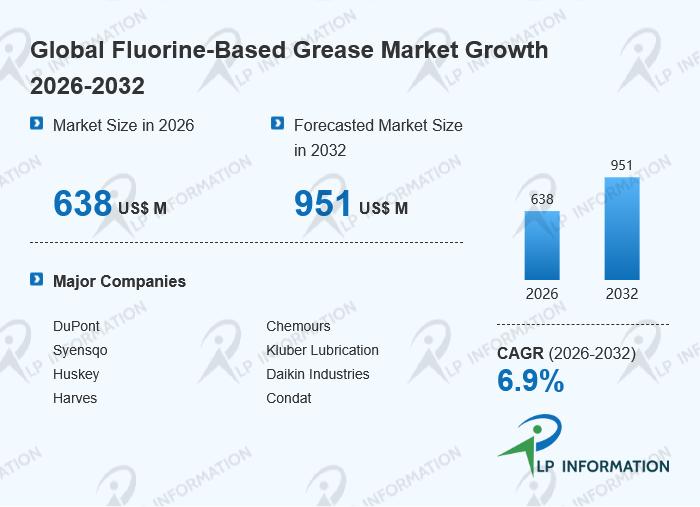
Fluorine-Based Grease Market to Reach US$951 Million by 2032, Growing at 6.9% CA …
Product Overview and Scope of Fluorine-Based Grease
Fluorinated lubricants are special grade synthetic lubricants, which possess superior properties as compared to petroleum based lubricants. Most of the petroleum based lubricants fail to perform under -18 °C and above 100 °C; the fluorinated lubricants can effectively perform between -90°C and 300 °C. Apart from extensive temperature endurance, significant endurance under high load conditions, hydrophobic nature, chemical inertness, oxidation resistant, etc. are some…

Copper Phosphorus Alloy Market to Reach US$688 Million by 2032, Growing at 6.7% …
Product Overview and Scope of Copper Phosphorus Alloy
Copper-phosphorus alloy (often sold as "phosphor copper" or CuP master alloy) is a specialty additive used primarily in foundries and metalworking plants to introduce phosphorus into molten copper or copper alloys in a controlled, high-recovery way. Its main role is deoxidation-phosphorus reacts strongly with dissolved oxygen and helps reduce oxide-related defects-while it also serves as a composition adjuster when making phosphorus-containing alloys such…

Automated High-Temp Pressure Reactors Control Systems Market to Grow at 8.4% CAG …
The global market for Automated High-Temperature Pressure Reactors Control Systems is poised for significant growth, according to the latest industry research report covering the forecast period from 2025 to 2031 by LP Information. The market size, valued at USD 823 million in 2024, is projected to reach USD 1,447 million by 2031, growing at a compound annual growth rate (CAGR) of 8.4%.
Leading Companies
Major manufacturers contributing to the market's growth…

Balance Rehabilitation Trainer Market to Grow at 9.2% CAGR Through 2031
Balance Rehabilitation Trainer Market to Grow at 9.2% CAGR Through 2031
The global Balance Rehabilitation Trainer market, valued at USD 583 million in 2024, is forecast to reach USD 1,080 million by 2031, growing at a compound annual growth rate (CAGR) of 9.2% from 2025 to 2031. This strong growth reflects increased demand for neurological, orthopedic, and geriatric rehabilitation solutions amid global aging populations and rising incidence of stroke and…
More Releases for D2W
Hybrid Bonding Market Global Demand Analysis and Forecast 2026 to 2035
InsightAce Analytic Pvt. Ltd. announces the release of a market assessment report on the "Global Hybrid Bonding Market Size, Share & Trends Analysis Report By Equipment Type (Wafer Bonders, Surface Prep Tools, Inspection & Metrology Tools, and Cleaning & CMP Systems), Bonding Type (Copper-to-Copper (Cu-Cu), Copper-to-Pad/Metal-to-Pad, and Others), Integration Level (2.5D Packaging, 3D Stacked Ics, and Heterogeneous Integration), Process Flow (Front-end and Back-end), Application (Memory & Storage, Computing & Logic,…
Global Advanced Bonding Equipment Market Analysis: Capturing the 7.5% CAGR Surge …
Global Leading Market Research Publisher QYResearch announces the release of its latest report "Advanced Bonding Equipment - Global Market Share and Ranking, Overall Sales and Demand Forecast 2026-2032".
The semiconductor industry stands at a pivotal inflection point where traditional Moore's Law scaling confronts escalating physical and economic barriers. As device geometries approach atomic dimensions, the strategic imperative has decisively shifted from monolithic transistor shrinkage toward heterogeneous integration and 3D stacking-architectural paradigms…
Hybrid Bonding Die Bonder Market Outlook 2026-2032: Ultra-Precision Packaging Eq …
Hybrid Bonding Die Bonder Market Forecast 2026-2032: Ultra-Precision Packaging Equipment Driving 3D IC, HBM, and Advanced Semiconductor Integration
Global Leading Market Research Publisher QYResearch announces the release of its latest report "Hybrid Bonding Die Bonder - Global Market Share and Ranking, Overall Sales and Demand Forecast 2026-2032". Based on current situation and impact historical analysis (2021-2025) and forecast calculations (2026-2032), this report provides a comprehensive analysis of the global Hybrid Bonding…
Hybrid Bonding Market Value Chain and Forecast Analysis 2026 to 2035
InsightAce Analytic Pvt. Ltd. announces the release of a market assessment report on the "Global Hybrid Bonding Market Size, Share & Trends Analysis Report By Equipment Type (Wafer Bonders, Surface Prep Tools, Inspection & Metrology Tools, and Cleaning & CMP Systems), Bonding Type (Copper-to-Copper (Cu-Cu), Copper-to-Pad/Metal-to-Pad, and Others), Integration Level (2.5D Packaging, 3D Stacked Ics, and Heterogeneous Integration), Process Flow (Front-end and Back-end), Application (Memory & Storage, Computing & Logic,…
Segment Evaluation and Major Growth Areas in the Wafer Bonder and Debonder Marke …
The wafer bonder and debonder market is positioned for significant expansion as demand for advanced semiconductor packaging intensifies. With technological advancements and increasing applications across various high-tech industries, the market is expected to experience robust growth over the coming years. Let's examine the market's size forecast, key players, emerging trends, and segmentation to understand the industry's trajectory.
Projected Growth and Market Size of the Wafer Bonder and Debonder Industry
The wafer…
Hybrid Bonding Market: The "Bumpless" Revolution Enabling the Future of 3D Stack …
The Hybrid Bonding Market is rapidly emerging as the single most critical technology for extending Moore's Law in the era of Artificial Intelligence and High-Performance Computing (HPC). As traditional micro-bump interconnects hit physical scaling limits, the semiconductor industry is pivoting to Hybrid Bonding-a bumpless, copper-to-copper bonding technique that enables vertical stacking of chips with unprecedented density and bandwidth. This technology, originally commercialized in image sensors, is now becoming the standard…

