


Press release
Stanford Advanced Materials Expands Epi-Ready Sapphire Wafer Portfolio to 8-Inch Diameters
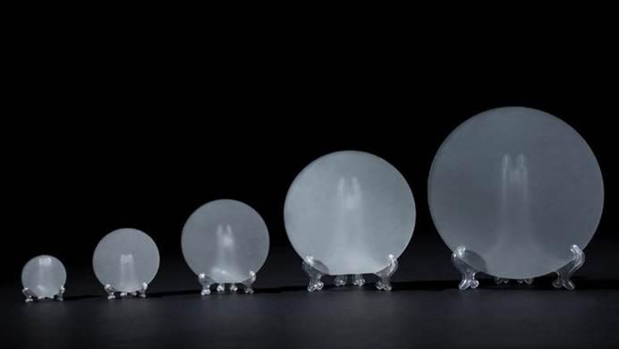
Image: https://www.globalnewslines.com/uploads/2026/08/4de629bb380e3b7bdea949fbf29e3a81.jpg
Santa Ana, United States - August 26, 2026 - Addressing Technical Challenges: Thermal Mismatch and Defect Rates in Large-Diameter Sapphire Substrates
As manufacturers move toward larger substrate formats, wafer flatness, surface quality, crystal orientation, and consistency become increasingly important to epitaxial process control.
Sapphire wafers are a core substrate material in LEDs, optoelectronics, and power semiconductors. As Mini-LEDs, Micro-LEDs, and next-gen power devices push for larger wafer sizes, the industry is transitioning from 2inch and 4inch to 6inch and even 8inch formats.
But scaling up comes with serious technical challenges. Research shows that due to the thermal expansion mismatch between sapphire and gallium nitride (GaN), larger sapphire wafers face a significantly higher risk of warpage and cracking. As sapphire wafer diameter increases, controlling bow, warp, total thickness variation, and surface quality becomes more demanding. In GaN epitaxy, lattice and thermal expansion mismatch between GaN and sapphire can also contribute to residual stress in the epitaxial structure.
For research institutions and high-reliability device makers, what's really needed is a sapphire wafer that delivers high purity, low defect density, precise crystal lattice orientation, and customization options-all while helping them dodge the yield pitfalls that come with mass production.
High-Purity Sapphire Wafers Built for High-End Applications
Stanford Advanced Materials offers sapphire wafers [https://www.samaterials.com/aluminum/2173-sapphire-wafer.html] with purity up to 99.999%, meeting the most demanding semiconductor process requirements.
Superior Mohs 9 Hardness for Harsh Semiconductor Environments
Sapphire ranks 9 on the Mohs scale-right behind diamond. That gives it outstanding scratch resistance and long-term durability, preserving surface integrity even in aggressive processing environments. This makes it not only an ideal LED substrate but also a solid choice for precision mechanical parts and vacuum equipment.
High Thermal and Dimensional Stability
Sapphire combines high-temperature stability with good dimensional integrity and electrical insulation, making it suitable for demanding epitaxial growth and semiconductor processing environments.
Broad Optical Transmission (0.2-4m) and High Dielectric Strength
Sapphire delivers excellent transmission from UV to infrared (0.2-4m), and its wide bandgap makes it a great electrical insulator. This combination of optical transparency and electrical insulation gives it unique value in optoelectronics and sensor applications.
Chemical Inertness Against Etching and Plasma Clean Processes
Sapphire offers strong chemical stability against many processing chemicals used in semiconductor and laboratory environments. Its chemical durability can help maintain substrate integrity and reduce contamination risks during compatible processing steps.
Customizable Crystal Orientations (C, A, R, M Planes) and Epi-Ready Specifications
Sapphire wafers are anisotropic, different crystal orientations deliver different optical, mechanical, and electrical properties. Stanford Advanced Materials typically offers a range of standard orientations, including Cplane (0001), Aplane (1120), Rplane (1102), and Mplane (1010). Cplane sapphire wafers are the goto choice for GaNbased LED and power device epitaxy, while Rplane is often used for specialized applications like silicononsapphire (SOS) wafers.
As for sizes, we cover diameters from 1 inch up to 8 inches, with thickness customizable from 0.35mm to 1mm. For GaN epitaxy and similar applications, singleside or doubleside polished (DSP) sapphire wafers are available, with surface roughness down to Ra less than or equal to 5 A, meeting EpiReady standards.
Dr. Samuel R. Matthews, Chief Materials Officer at Stanford Advanced Materials, commented: "The quality of the sapphire wafer directly determines the crystalline integrity of the epitaxial layer and, ultimately, device performance. Our sapphire wafers are built around that very principle-to give our customers reliable materials that help reduce substraterelated losses, whether they're in R&D or volume production."
About Stanford Advanced Materials
Stanford Advanced Materials (SAM) [https://www.samaterials.com/] is a global supplier of highpurity materials, offering a wide range of crystalline substrates including sapphire wafers for the semiconductor, optoelectronics, optics, and scientific research communities. With a broad customer base, SAM's sapphire wafers are used not only in LED and power device development but also in consumer electronics and aerospace applications. Looking for custom dimensions or Epi-Ready substrates for your next R&D project? Request a Quote for SAM Sapphire Wafers.
Media Contact
Company Name: Stanford Advanced Materials
Contact Person: Maria Higgins
Email: Send Email [http://www.universalpressrelease.com/?pr=stanford-advanced-materials-expands-epiready-sapphire-wafer-portfolio-to-8inch-diameters]
City: Santa Ana
Country: United States
Website: http://www.samaterials.com
Legal Disclaimer: Information contained on this page is provided by an independent third-party content provider. GetNews makes no warranties or responsibility or liability for the accuracy, content, images, videos, licenses, completeness, legality, or reliability of the information contained in this article. If you are affiliated with this article or have any complaints or copyright issues related to this article and would like it to be removed, please contact retract@swscontact.com
This release was published on openPR.
Permanent link to this press release:
Copy
Please set a link in the press area of your homepage to this press release on openPR. openPR disclaims liability for any content contained in this release.
You can edit or delete your press release Stanford Advanced Materials Expands Epi-Ready Sapphire Wafer Portfolio to 8-Inch Diameters here
News-ID: 4614496 • Views: …
More Releases from Getnews

The "The Most Beautiful Scenery is on the Road, Explore the Splendor of Hebei" t …
Beijing - August 26, 2026 - Recently, the "The Most Beautiful Scenery is on the Road - Explore the Scenery of Hebei" themed tour, jointly organized by the Hebei Provincial Department of Culture and Tourism and China Cultural Media Group, and undertaken by Zhongchuan Global (Beijing) New Media Technology Co., Ltd., successfully concluded.
Image: https://www.globalnewslines.com/uploads/2026/08/466ca583d9fd60e380aa7b6c17fa78bb.jpg
This event, themed around the three distinctive cultural and tourism corridors of the Taihang Mountains, the Grand…

KAPSTO Protective Elements Featured at Eight Industrial Trade Fairs This Autumn
Image: https://www.globalnewslines.com/uploads/2026/08/1787670271.jpg
Claremont, Germany - Aug 26, 2026 - The September-November 2026 exhibition calendar spans automotive supply, battery production, electronics, advanced manufacturing, and construction machinery - sectors where component protection during production, storage, and transport determines whether parts arrive fit for assembly
Poppelmann KAPSTO, a manufacturer of plastic protective caps, plugs, and thermoformed trays for industrial applications, is scheduled to appear at eight trade fairs between late September and late November 2026.…

Creative Biolabs Expands Specialized Exosome Isolation Services for Extracellula …
Creative Biolabs has expanded its custom exosome isolation platform to support extracellular vesicle research across complex biological matrices.
New York, USA - August 26, 2026 - Designed exclusively for academic and preclinical research, the expanded service portfolio addresses fundamental technical bottlenecks in extracting high-purity extracellular vesicles (EVs) from complex biological matrices. This structural enhancement provides researchers with scalable, reproducible vesicle populations necessary for advanced multi-omics profiling, biomarker discovery, and cargo delivery…

Disabled Veteran Entrepreneur Turns a Mother's Search for Answers Into a Global …
2X Concurrent Amazon Bestselling Author Matilda Tart Expands Blue Butterfly Publications with a First-of-Its-Kind Ecosystem of Inclusive Books, Cognitive Tools and Community Experiences.
Dallas, Texas, USA - August 26, 2026 - What began as one mother searching for better ways to support her neurodivergent child has grown into a mission designed to help families around the world find the resources, representation and support she once struggled to find.
Matilda Tart, U.S. Army…
More Releases for Sapphire
Nash Gems Showcases Rare Teal Sapphire, Blue Green Sapphire, Blue Sapphire, and …
Nash Gems, a luxury gemstone brand under Nashcraft LLC, is proud to present its extraordinary range of sapphires, including teal sapphire, blue green sapphire, blue sapphire, and pink sapphire, sourced directly from mines in Sri Lanka and Madagascar. With over three generations in the sapphire trade, Nash Gems has become a global destination for high-quality gemstones and bespoke jewelry at competitive prices.
For more than 40 years, the Nash family has…
Sapphire Tube And Sapphire Rod Market Size and Outlook by Application, Type, and …
According to Market Research Intellect, the global Sapphire Tube And Sapphire Rod market under the Internet, Communication and Technology category is expected to register notable growth from 2025 to 2032. Key drivers such as advancing technologies, changing consumer behavior, and evolving market dynamics are poised to shape the trajectory of this market throughout the forecast period.
The market for sapphire tubes and rods is expanding steadily as a result of the…
Sapphire Technology Market Boost with 42380.0 million $ Size Forecast to 2024 | …
Sapphire Technology Market report defines share, trends, growth, size, development in-detail from trusted industrial sources. Sapphire Technology Market will exhibit remarkable CAGRs in the aforementioned period 2020-2024.
Global Sapphire Technology Market Overview:
According to Market analyst Sapphire Technology industry has also suffered a certain impact, but still maintained a relatively optimistic growth, the past four years, Sapphire Technology market size to maintain the average annual growth rate of 0.0677151134699 from 17800.0 million…
Sapphire Technology Market 2017 - 2025 : Sapphire Technology Co. Ltd., Rubicon T …
Global Sapphire Technology Market: Snapshot
Sapphires are a type of gemstone formed based off a specific type of aluminum oxide. While they are typically blue in color, there are certain sapphires that can be found in other colors, such as orange or green, while some sapphires may even show two or more colors. There is a wide range of non-ornamental applications for sapphires and sapphire technology. Some of the key uses…
Sapphire Technology Global Market, 2017: By Application - Si-On-Sapphire, SiC-On …
Researchmoz added Most up-to-date research on "Sapphire Technology Global Market, 2017: By Application - Si-On-Sapphire, SiC-On-Sapphire, GaN-On-Sapphire & Others" to its huge collection of research reports.
This report studies Sapphire Technology in Global market, especially in North America, Europe, China, Japan, Korea and Taiwan, focuses on top manufacturers in global market, with capacity, production, price, revenue and market share for each manufacturer, covering
GT Advanced Technology
Rubicon Technology
Namiki Precision Jewel Co
Monocrystal Inc
DK Aztec…
2024 Sapphire Substrates Market Prediction
Global Sapphire Substrates Market: Overview
This report provides strategic study of the global sapphire substrates market, and the growth forecast for the period 2016 to 2024. The scope of the report includes competitive analysis of various market segments based on wafer diameter, applications, and in-depth cross-sectional scrutiny of the sapphire substrates market across different geographical segments. Sapphire is considered as a gemstone. Its chemical formula is Al2O3 and is a type…

