


Press release
Semiconductor Advanced Substrate Market to Reach US$23 Billion by 2033 at 10.3% CAGR
Semiconductor Advanced Substrate Market
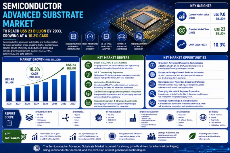
Advanced semiconductor substrates are becoming increasingly important as chip architectures evolve toward higher levels of integration and computational density. The expansion of generative AI, machine learning, cloud computing, hyperscale data centers, 5G infrastructure, autonomous vehicles, and high-performance computing is increasing the need for sophisticated packaging technologies capable of supporting increasingly complex semiconductor devices. Advanced substrates such as ABF substrates, BT substrates, FC-BGA, FC-CSP, and emerging glass substrates are therefore becoming critical components in the semiconductor packaging ecosystem.
Get Your FREE Sample Report Instantly - Click Now: https://www.persistencemarketresearch.com/samples/37182
Market Segmentation
The semiconductor advanced substrate market can be segmented by substrate type into ABF substrate, BT substrate, FC-BGA, FC-CSP, and glass substrate. ABF substrates are particularly important for high-performance computing applications because they support high-density interconnections and fine-line packaging architectures. BT substrates continue to serve a broad range of semiconductor packages, while FC-BGA and FC-CSP are widely used in applications requiring high electrical performance and compact package designs. Glass substrates represent an emerging category that is attracting attention for next-generation semiconductor packaging because of their dimensional stability and potential to support increasingly dense interconnect structures.
Based on packaging technology, the market is divided into 2D packaging, 2.5D packaging, and 3D IC packaging. Conventional 2D packaging remains important across established semiconductor applications, but 2.5D packaging is gaining momentum for AI accelerators, GPUs, HPC processors, and networking devices because it enables multiple chiplets or dies to be integrated on an advanced substrate or interposer architecture. 3D IC packaging is expected to gain importance as semiconductor manufacturers pursue greater integration and performance while overcoming physical scaling limitations.
By material, the market is categorized into organic, ceramic, and glass materials. Organic substrates remain widely adopted because of their scalability, manufacturing maturity, and cost advantages. Ceramic substrates provide favorable thermal and electrical characteristics for specialized applications, including high-performance and demanding electronic environments. Glass is emerging as a next-generation substrate material, particularly for advanced packaging architectures requiring high dimensional stability and fine-pitch interconnections.
Based on end use, the market includes AI accelerators, CPUs, GPUs, networking chips, automotive semiconductors, and others. AI accelerators and GPUs are expected to remain major growth drivers due to increasing computational requirements from generative AI, machine learning, data analytics, and HPC. CPUs and networking chips also require advanced substrates to support higher performance and greater integration. Automotive semiconductors represent another important opportunity as electric vehicles, advanced driver-assistance systems, autonomous driving, and software-defined vehicles increase semiconductor content.
By industry, the market is segmented into consumer electronics, automotive, data centers, telecommunications, and others. Data centers are expected to represent one of the strongest demand centers as AI workloads and cloud computing drive investments in advanced processors and accelerators. Consumer electronics continue to require smaller and more powerful semiconductor packages, while telecommunications applications benefit from advanced chips for 5G networks and high-speed connectivity. Automotive applications are expanding as vehicles incorporate increasingly sophisticated electronic control, sensing, computing, and connectivity systems.
Regional Insights
North America represents an important market for semiconductor advanced substrates due to its strong semiconductor design ecosystem, growing AI infrastructure investments, and rapidly expanding data center capacity. The United States is a major demand center for AI accelerators, GPUs, HPC processors, networking chips, and cloud infrastructure. Investments by hyperscale data center operators and technology companies are increasing demand for advanced semiconductor packaging, creating opportunities throughout the substrate supply chain.
Asia Pacific is expected to remain a dominant region in the semiconductor advanced substrate industry because of its extensive semiconductor manufacturing and electronics ecosystem. Countries including Taiwan, South Korea, Japan, and China have significant capabilities across semiconductor fabrication, packaging, substrates, materials, and electronics manufacturing. The region's strong presence in advanced packaging and growing investments in AI chips, consumer electronics, automotive semiconductors, and data center infrastructure are expected to support sustained market growth.
Japan has a particularly strong position in advanced semiconductor substrates due to its established expertise in high-end materials, packaging technologies, and substrate manufacturing. Companies such as Ibiden Co., Ltd., Shinko Electric Industries Co., Ltd., and Kyocera Corporation contribute to the region's advanced packaging ecosystem. South Korea also remains strategically important because of its leadership in memory, semiconductor manufacturing, electronics, and advanced packaging technologies.
Europe represents another important market, particularly for automotive semiconductors, industrial electronics, telecommunications, and high-performance computing. The region's automotive industry is driving demand for advanced semiconductor packaging as electric vehicles and autonomous driving systems increase semiconductor content. European substrate manufacturers and technology companies are also investing in advanced packaging capabilities to strengthen regional semiconductor supply chains.
Do You Have Any Query Or Specific Requirement? Request Customization of Report: https://www.persistencemarketresearch.com/request-customization/37182
Market Drivers
The rapid expansion of artificial intelligence and generative AI is one of the strongest drivers of the semiconductor advanced substrate market. AI workloads require powerful accelerators, GPUs, high-bandwidth memory, networking processors, and sophisticated computing architectures. These devices generate substantial amounts of data and require advanced packaging solutions capable of supporting high bandwidth, dense interconnections, improved signal integrity, and efficient thermal management.
The expansion of hyperscale data centers and high-performance computing infrastructure is another major growth factor. Cloud service providers and technology companies are investing heavily in computing infrastructure to support AI training, inference, cloud applications, data analytics, and enterprise workloads. Advanced substrates are critical for packaging the high-performance chips used within these systems.
The growing adoption of chiplet architectures and advanced packaging is further supporting demand. Instead of relying solely on increasingly large monolithic dies, semiconductor designers are increasingly combining multiple chiplets or functional dies within a single package. This approach requires advanced substrate technologies capable of handling high-density interconnections and complex electrical architectures.
Market Restraints
The semiconductor advanced substrate market faces challenges associated with high manufacturing costs and technological complexity. Advanced substrates require sophisticated manufacturing equipment, highly precise processes, specialized materials, and stringent quality control. These requirements can increase production costs and create significant barriers for new market participants.
Another restraint is the complexity of supply chains for semiconductor packaging materials and equipment. Advanced substrate manufacturing depends on specialized raw materials, manufacturing tools, chemicals, and precision equipment. Disruptions across any part of the supply chain can affect production schedules and increase costs.
The industry also faces challenges related to manufacturing yield and capacity constraints. Advanced packaging substrates require extremely precise fabrication processes, particularly for high-density and fine-line applications. As demand for AI chips and HPC processors increases rapidly, manufacturers must expand capacity while maintaining quality and yield levels.
Market Opportunities
The rapid adoption of 2.5D and 3D packaging technologies presents significant opportunities for substrate manufacturers. These architectures allow semiconductor companies to integrate multiple components within compact packages and improve communication between dies. As AI accelerators and HPC processors become more complex, demand for substrates capable of supporting these architectures is expected to increase.
Glass substrate technology represents another significant long-term opportunity. Glass offers attractive properties for advanced packaging, including high dimensional stability and potential compatibility with fine-pitch interconnections. As semiconductor manufacturers seek alternatives and complementary solutions to conventional organic substrates, investment in glass-based packaging technologies could accelerate.
The increasing localization of semiconductor supply chains also creates opportunities for substrate manufacturers across North America, Europe, and Asia. Governments and semiconductor companies are investing in domestic manufacturing capabilities to reduce supply chain vulnerabilities. This trend can encourage new advanced packaging facilities, partnerships, technology transfers, and capacity expansions.
Secure Your Full Report - Proceed to Checkout: https://www.persistencemarketresearch.com/checkout/37182
Frequently Asked Questions (FAQs)
How Big is the Global Semiconductor Advanced Substrate Market?
Who are the Key Players in the Global Semiconductor Advanced Substrate Market?
What is the Projected Growth Rate of the Semiconductor Advanced Substrate Market?
What is the Market Forecast for the Semiconductor Advanced Substrate Market by 2033?
Which Region is Estimated to Dominate the Semiconductor Advanced Substrate Industry through the Forecast Period?
Company Insights
The global semiconductor advanced substrate market features established substrate manufacturers, electronics companies, advanced materials suppliers, and semiconductor packaging specialists. Leading companies are focusing on expanding production capacity, developing finer-line substrates, improving manufacturing yields, and supporting advanced packaging architectures for AI and high-performance computing.
• Ibiden Co., Ltd.
• Samsung Electro-Mechanics Co., Ltd.
• AT&S (Austria Technologie & Systemtechnik AG)
• Shinko Electric Industries Co., Ltd.
• Unimicron Technology Corporation
• Nan Ya Printed Circuit Board Corporation
• Kyocera Corporation
• Corning Incorporated
Recent Developments
Advanced packaging capacity expansion: Leading substrate manufacturers are continuing to invest in advanced packaging substrate production to address growing demand from AI accelerators, GPUs, HPC processors, and data center applications.
Growth of glass substrate technology: Semiconductor and materials companies are advancing glass-based substrate technologies for next-generation packaging, focusing on dimensional stability, high-density interconnections, and the requirements of increasingly complex semiconductor architectures.
Conclusion
The global semiconductor advanced substrate market is positioned for strong expansion, increasing from US$11.6 billion in 2026 to US$23 billion by 2033 at a CAGR of 10.3%. The market's growth is being driven primarily by the rapid development of AI accelerators, GPUs, HPC processors, advanced networking chips, and data center infrastructure.
As semiconductor architectures become increasingly complex, advanced substrates are becoming a critical component in delivering higher computing performance, greater interconnect density, improved thermal management, and smaller package footprints. The continued adoption of 2.5D and 3D packaging, chiplet architectures, ABF substrates, and emerging glass substrate technologies will create significant opportunities across the semiconductor packaging ecosystem.
With AI infrastructure investment accelerating and semiconductor supply chains undergoing strategic transformation, substrate manufacturers that can deliver high-quality, high-density, and scalable packaging solutions are likely to benefit substantially. The convergence of advanced packaging innovation, AI computing, data center expansion, and next-generation semiconductor architectures will remain a key force shaping the market through 2033.
Related Reports:
Mobile Advertising Market https://www.persistencemarketresearch.com/market-research/mobile-advertising-market.asp
Optical Power Meter Market https://www.persistencemarketresearch.com/market-research/optical-power-meter-market.asp
AI Consulting Services Market https://www.persistencemarketresearch.com/market-research/ai-consulting-services-market.asp
Contact Us:
Persistence Market Research
Second Floor, 150 Fleet Street,
London, EC4A 2DQ, United Kingdom
USA Phone: +1 646-878-6329
UK Phone: +44 203-837-5656
Email: sales@persistencemarketresearch.com
Web: https://www.persistencemarketresearch.com
About Persistence Market Research:
At Persistence Market Research, we specialize in creating research studies that serve as strategic tools for driving business growth. Established as a proprietary firm in 2012, we have evolved into a registered company in England and Wales in 2023 under the name Persistence Research & Consultancy Services Ltd. With a solid foundation, we have completed over 3600 custom and syndicate market research projects, and delivered more than 2700 projects for other leading market research companies' clients.
Our approach combines traditional market research methods with modern tools to offer comprehensive research solutions. With a decade of experience, we pride ourselves on deriving actionable insights from data to help businesses stay ahead of the competition. Our client base spans multinational corporations, leading consulting firms, investment funds, and government departments. A significant portion of our sales comes from repeat clients, a testament to the value and trust we've built over the years.
This release was published on openPR.
Permanent link to this press release:
Copy
Please set a link in the press area of your homepage to this press release on openPR. openPR disclaims liability for any content contained in this release.
You can edit or delete your press release Semiconductor Advanced Substrate Market to Reach US$23 Billion by 2033 at 10.3% CAGR here
News-ID: 4605606 • Views: …
More Releases from Persistence Market Research
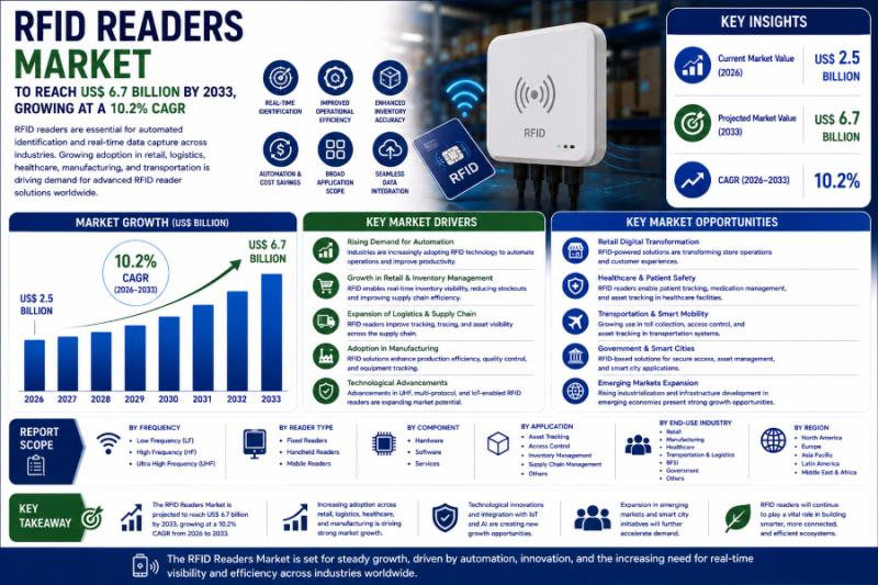
RFID Readers Market to Reach US$6.7 Billion by 2033, Growing at a 10.2% CAGR fro …
The global RFID readers market size is likely to be valued at US$3.4 billion in 2026 and is expected to reach US$6.7 billion by 2033, growing at a CAGR of 10.2% during the forecast period from 2026 to 2033. Market growth is being driven by increasing investments in automated identification, real-time asset tracking, inventory visibility, and connected supply chains across retail, logistics, manufacturing, healthcare, transportation, and other industries. RFID readers…
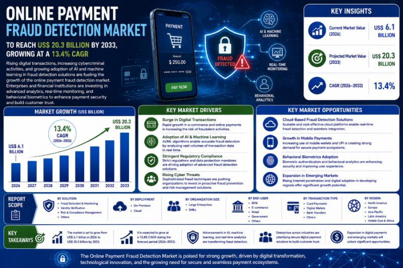
Online Payment Fraud Detection Market to Reach US$20.3 Billion by 2033 at 13.4% …
The global Online Payment Fraud Detection market size is expected to be valued at US$8.4 billion in 2026 and is projected to reach US$20.3 billion by 2033, growing at a CAGR of 13.4% between 2026 and 2033. The market is expanding rapidly as digital payments, mobile commerce, online banking, and card-not-present transactions become increasingly prevalent worldwide. The growing sophistication of cybercriminals, rising financial losses associated with payment fraud, and increasing…
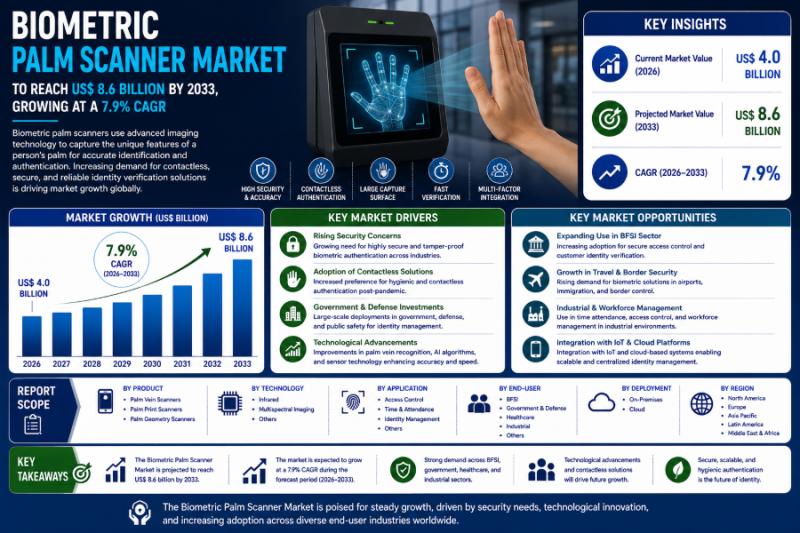
Biometric Palm Scanner Market to Reach US$8.6 Billion by 2033, Growing at a 7.9% …
The global biometric palm scanner market size is likely to be valued at US$5.1 billion in 2026 and is estimated to reach US$8.6 billion by 2033, growing at a CAGR of 7.9% during the forecast period from 2026 to 2033. Market growth is being supported by increasing demand for contactless authentication, rising concerns regarding identity security, growing adoption of biometric access control, and the need for reliable identification across healthcare,…
Solar Powered Camera Market to Reach US$23.1 Billion by 2033, Growing at 12.1% C …
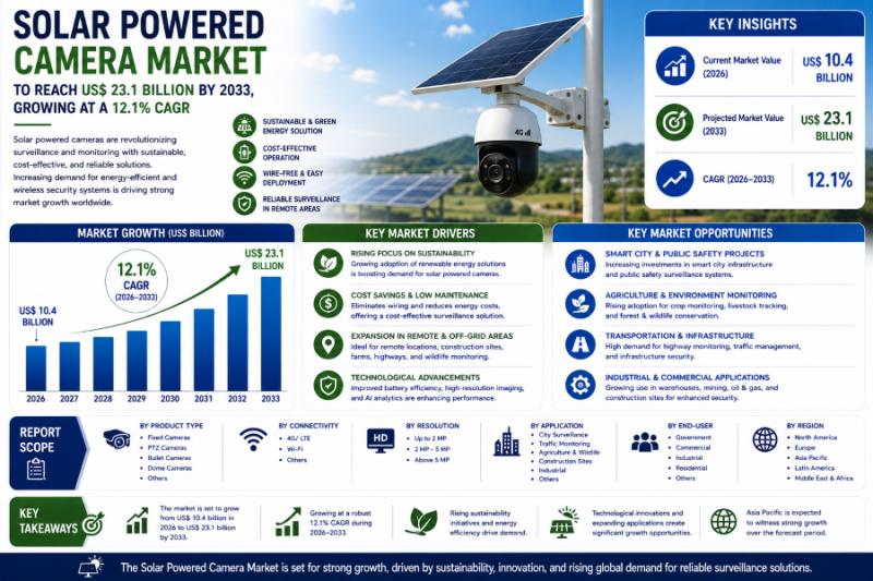
The global solar powered camera market size is expected to be valued at US$10.4 billion in 2026 and is projected to reach US$23.1 billion by 2033, growing at a CAGR of 12.1% between 2026 and 2033. Market growth is being supported by rising demand for remote surveillance, increasing adoption of wireless security systems, expanding smart city initiatives, and the need for reliable security solutions in locations where conventional grid power…
More Releases for Advanced
Advanced Oxidation Technologies Market Size, Share 2021, Impressive Industry Gro …
The Advanced Oxidation Technologies Market is poised to take off in upcoming years hence showing a highly positive outlook through 2020-2028, according to a recently released report. Advanced Oxidation Technologies Market report covers industry chain analysis, latest market trends & dynamics along with cost profit analysis of major key players which focuses on expansion rate, prices, competition, size, prices, and value chain analysis of those leaders in the market.
The…
Medical Ceramics Market Analysis and Industry Forecast | Advanced Ceramics Resea …
Allied Market Research published a new report, titled, “Medical Ceramics Market by Type (Aluminum Oxide, Zirconia, and Carbon, Hydroxyapatite, Glass & Bioglass, Zirconia Alumina, Bioresorbable Ceramics, and Piezo Ceramics), by Application (Surgical Instruments, Diagnostic Equipment, Orthopedic Implants, Electronic Implants, Dental Implants, Disposables, and Packaging) – Global Opportunity Analysis and Industry Forecast, 2014 – 2022.” The report offers an extensive analysis of key growth strategies, drivers, opportunities, key segment, Porter’s Five…
Skincell Advanced Reviews – Does Skincell Advanced Really Work?
People want clear, blemish-free skin! However, most people have skin tags, moles, and warts. Some causes are known, while some blemishes are caused without any reason at all. When a regular skincare regimen fails, people turn to costly surgeries and medications. Cleansing and moisturizing might not work well for all. All skin types are not the same, and toners and skincare creams seldom give long-lasting benefits.
Get Skincell Advanced From Its…
Global Advanced Oxidation Technologies Market 2019- 2025 || A-Zone Technologies, …
Synopsis of the Advanced Oxidation Technologies Market:
Latest Report on Advanced Oxidation Technologies Market deliberates the effect of various Factors influencing the market growth and drivers. Its further sheds light on market overview, key manufacturers, strategic adopted by them, size, latest trends and types, revenue, gross margin with regional analysis and forecast to 2025.
Overview of the Advanced Oxidation Technologies Market Report:
Advanced Oxidation Technologies Market report includes knowledge about the market overview…
Global Advanced Materials Market - 3M Company, DowDuPont Inc, Hexcel Corporation …
A New fresh research report presented by KD Market Insights provides a detailed analysis of “Advanced Materials Market - By Product type (Structural Material, Functional Material, Emerging Material) By End User (Building & Construction, Automotive, Aerospace, Defense, Marine, Electrical & Electronics, Healthcare, Oil & Gas and Energy, Others) & Global Region - Market Size, Trends, Share and Forecast 2018-2023” research report will include all the major trends and technologies that…
Global Advanced Materials Market: 3M Company, DowDuPont Inc, Hexcel Corporation, …
A New fresh research report presented by KD Market Insights provides a detailed analysis of “Advanced Materials Market 2017: Market Size, Trends & Opportunity Outlook – Forecast to 2023” research report will include all the major trends and technologies that play an important role in market growth in the predicted span of 6 years. It also presents the overview of industry players, advantages, challenges the business is going through. The…

