


Press release
Through-Silicon Via (TSV) Technology Market Growth Analysis 2026-2035 | USD 26.35 Billion Opportunity Driven by AI, High-Bandwidth Memory, 3D ICs & Advanced Semiconductor Packaging
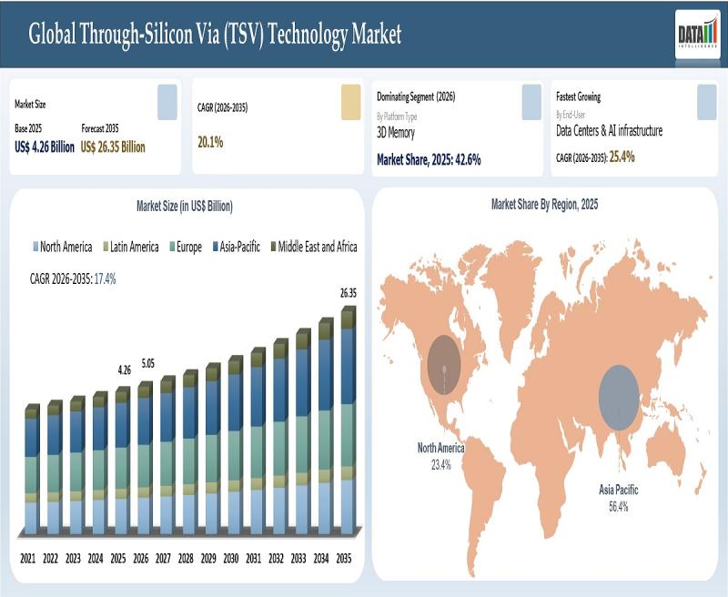
Through-Silicon Via (TSV) Technology Market
The market is also benefiting from continuous advancements in semiconductor packaging technologies, particularly 2.5D interposer and 3D TSV architectures, which enable enhanced processing capabilities and higher integration densities. 2.5D TSV packaging currently holds a significant share due to its cost effectiveness, scalability, and reliability, especially for AI accelerators and high performance computing applications, while 3D TSV packaging is expected to witness the fastest growth due to its superior bandwidth and improved system performance. Additionally, increasing investments in next generation semiconductor manufacturing, rising adoption of high-bandwidth memory (HBM), and growing demand for advanced computing platforms are expected to create substantial long term growth opportunities for the Through-Silicon Via (TSV) technology market globally during the forecast period.
Get a Free Sample PDF Of This Report (Get Higher Priority for Corporate Email ID): https://www.datamintelligence.com/download-sample/through-silicon-via-tsv-technology-market?sai-v
Key Developments
April 2026: The United States increased investments in advanced semiconductor packaging technologies, including Through-Silicon Via (TSV) solutions, to support high-performance computing, AI accelerators, and next-generation chip manufacturing capabilities.
March 2026: Japan accelerated research and development activities in 3D semiconductor integration, advanced wafer processing, and TSV manufacturing technologies to enhance chip performance, miniaturization, and energy efficiency.
February 2026: Leading semiconductor companies increased investments in TSV-based 2.5D and 3D packaging technologies, advanced interconnect architectures, and heterogeneous integration solutions for AI, data centers, and high-speed computing applications.
January 2026: Governments worldwide strengthened semiconductor supply chain initiatives and funding programs, supporting advanced packaging infrastructure, domestic chip production, and innovation in TSV-enabled semiconductor technologies.
December 2025: Major semiconductor manufacturers expanded collaborations with foundries, packaging companies, and material suppliers to accelerate the commercialization of high-density TSV solutions for memory, logic, and sensor applications.
November 2025: Semiconductor equipment providers increased development of precision etching, wafer bonding, and inspection technologies to improve TSV manufacturing efficiency, yield, and reliability for next-generation electronic devices.
Key Players
Taiwan Semiconductor Manufacturing Company Limited (TSMC) | Samsung Electronics | Intel Corporation | GlobalFoundries | United Microelectronics Corporation (UMC) | STMicroelectronics | SK hynix Inc. | Micron Technology, Inc. | Nanya Technology Corporation | Amkor Technology | Powertech Technology Inc. | Applied Materials, Inc. | ams-OSRAM AG | Others
Key Highlights
Taiwan Semiconductor Manufacturing Company Limited (TSMC) - Holds a 16.2% share, driven by its leadership in advanced semiconductor manufacturing, large-scale 3D IC packaging capabilities, and extensive adoption of Through-Silicon Via (TSV) technologies for high-performance computing and AI applications.
Samsung Electronics - Holds a 14.7% share, supported by its advanced memory and logic semiconductor technologies, HBM development, and strong investments in next-generation 3D packaging solutions utilizing TSV architecture.
Intel Corporation - Holds a 12.4% share, strengthened by its advanced packaging platforms, including Foveros 3D stacking technology, extensive R&D capabilities, and growing demand for high-performance semiconductor solutions.
GlobalFoundries - Holds a 9.3% share, fueled by its specialized semiconductor manufacturing services, advanced packaging technologies, and strategic collaborations across automotive, communications, and industrial applications.
United Microelectronics Corporation (UMC) - Holds a 7.8% share, supported by its mature process technologies, semiconductor manufacturing expertise, and expanding advanced packaging capabilities.
STMicroelectronics - Holds a 6.5% share, driven by its MEMS sensors, automotive semiconductors, and advanced integration technologies incorporating TSV solutions.
SK hynix Inc. - Holds a 6.1% share, strengthened by its leadership in HBM and DRAM technologies, advanced memory stacking capabilities, and increasing demand from AI data centers.
Micron Technology, Inc. - Holds a 5.8% share, supported by its innovative memory solutions, 3D packaging developments, and investments in high-bandwidth memory technologies.
Nanya Technology Corporation - Holds a 4.7% share, fueled by its DRAM manufacturing expertise, memory technology advancements, and development of high-performance semiconductor solutions.
Amkor Technology - Holds a 4.2% share, driven by its advanced semiconductor packaging and test services, including TSV-based 2.5D and 3D integration solutions.
Powertech Technology Inc. - Holds a 3.6% share, supported by its semiconductor assembly, testing services, advanced memory packaging expertise, and TSV integration capabilities.
Applied Materials, Inc. - Holds a 3.1% share, strengthened by its semiconductor manufacturing equipment, TSV fabrication technologies, and process innovation for advanced chip packaging.
ams-OSRAM AG - Holds a 2.4% share, driven by its advanced optical sensors, microelectronics expertise, and adoption of TSV technologies in compact semiconductor devices.
Others - Hold a combined 3.2% share, comprising emerging semiconductor foundries, packaging service providers, equipment manufacturers, and specialized technology companies advancing TSV-based 3D integration solutions.
Purchase Corporate License | Market Intelligence: https://www.datamintelligence.com/buy-now-page?report=through-silicon-via-tsv-technology-market?sai-v
Market Drivers
Increasing demand for high-performance computing, artificial intelligence, data centers, and advanced semiconductor packaging solutions is significantly driving growth of the Through-Silicon Via (TSV) technology market worldwide.
Growing adoption of 3D integrated circuits (3D ICs), heterogeneous integration, and advanced chip stacking technologies is accelerating demand for TSV solutions across semiconductor applications.
Rising requirements for smaller, faster, and energy-efficient electronic devices are strengthening the need for high-density interconnect technologies and advanced semiconductor architectures.
Expansion of consumer electronics, smartphones, wearable devices, and high-performance computing systems is contributing to increased utilization of TSV-enabled semiconductor packages.
Increasing adoption of high-bandwidth memory (HBM), image sensors, MEMS devices, and advanced logic chips is supporting market expansion globally.
Continuous advancements in semiconductor manufacturing processes, wafer-level packaging, and 3D integration technologies are improving TSV performance, reliability, and production efficiency.
Growing investments from semiconductor manufacturers, foundries, and technology companies in advanced packaging facilities and next-generation chip development are accelerating innovation across the TSV ecosystem.
Rising demand for artificial intelligence accelerators, autonomous vehicles, 5G infrastructure, and edge computing applications is further propelling global Through-Silicon Via (TSV) technology market growth.
Industry Developments
Rapid advancement in 3D semiconductor packaging, chiplet architectures, and heterogeneous integration technologies improving performance, bandwidth, and power efficiency.
Increasing adoption of TSV-based high-bandwidth memory solutions and advanced packaging methods supporting next-generation computing applications.
Growing investments in semiconductor fabrication plants, advanced packaging facilities, and research initiatives accelerating innovation across the TSV technology ecosystem.
Expansion of TSV applications in image sensors, MEMS, RF devices, AI processors, and high-performance computing platforms improving long-term market opportunities.
Rising collaborations among semiconductor foundries, integrated device manufacturers, packaging companies, and research organizations driving development of advanced 3D integration technologies.
Strategic partnerships, capacity expansions, technology launches, and manufacturing process improvements supporting global market growth and commercialization.
Continuous innovation in wafer thinning, copper filling, thermal management, and TSV fabrication techniques improving chip performance, reliability, and cost efficiency.
Regional Insights
Asia Pacific 61.7% share: "Leads the market due to dominant semiconductor manufacturing capabilities, presence of major foundries and packaging companies, high electronics production volumes, and significant investments in advanced semiconductor technologies across Taiwan, South Korea, China, and Japan."
North America 21.5% share: "Growth supported by strong demand for AI processors, high-performance computing systems, advanced semiconductor research, and substantial investments in chip design and packaging technologies."
Europe 11.3% share: "Strong market presence driven by increasing semiconductor innovation, automotive electronics demand, and investments in advanced manufacturing capabilities."
Latin America 3.0% share: "Growth supported by expanding electronics manufacturing activities, increasing adoption of advanced semiconductor components, and gradual development of technology infrastructure."
Middle East & Africa 2.5% share: "Gradual growth driven by increasing digital transformation initiatives, rising investments in technology infrastructure, and growing demand for advanced electronic systems."
Speak to our analyst and get customization in the report as per your requirements: https://www.datamintelligence.com/customize/through-silicon-via-tsv-technology-market?sai-v
Key Segments
➥ By Process Type
Via First: Represents a significant segment, driven by its early integration of TSV structures during semiconductor wafer fabrication, enabling high-density interconnections and enhanced device performance.
Via Middle: Represents a rapidly growing segment, supported by its ability to balance manufacturing flexibility, cost efficiency, and improved electrical performance in advanced semiconductor packaging.
Via Last: Represents the dominant segment, fueled by its compatibility with existing CMOS manufacturing processes, lower production complexity, and increasing adoption in 3D integrated circuits and advanced packaging technologies.
➥ By Platform Type
3D Integrated Circuits (3D ICs): Represents the dominant segment, driven by increasing demand for high-performance computing, reduced power consumption, and greater functionality through vertical stacking of semiconductor dies.
2.5D Integrated Circuits (2.5D ICs): Represents a significant segment, supported by rising adoption in high-bandwidth memory, AI processors, and advanced computing applications requiring high-density interconnects.
3D Wafer-Level Packaging: Represents a growing segment, fueled by the increasing need for miniaturized electronic devices, improved thermal performance, and enhanced packaging efficiency.
Others: Represents a moderate segment, supported by ongoing innovations in heterogeneous integration and next-generation semiconductor packaging technologies.
➥ By Application
Memory Devices: Represents the dominant segment, driven by extensive use of TSV technology in high-bandwidth memory (HBM), DRAM stacking, and advanced memory architectures for AI, data centers, and high-performance computing.
CMOS Image Sensors: Represents a significant segment, supported by growing demand for high-resolution cameras in smartphones, automotive systems, and industrial imaging applications.
MEMS & Sensors: Represents a substantial segment, fueled by increasing adoption of miniaturized sensors in consumer electronics, healthcare devices, automotive technologies, and IoT applications.
LED Packaging: Represents a growing segment, driven by the need for compact, efficient, and high-performance lighting and display technologies.
Others: Represents a moderate segment, supported by expanding applications in RF devices, photonics, and advanced semiconductor components.
➥ By End-User
Consumer Electronics: Represents the dominant segment, driven by rising demand for compact, high-performance smartphones, tablets, wearable devices, and gaming systems utilizing advanced semiconductor packaging.
Automotive: Represents a significant segment, supported by increasing adoption of advanced driver assistance systems (ADAS), autonomous driving technologies, and connected vehicle electronics.
Healthcare: Represents a growing segment, fueled by expanding use of miniaturized medical devices, diagnostic equipment, and wearable healthcare technologies.
Industrial: Represents a substantial segment, driven by increasing implementation of automation, robotics, and IoT-enabled systems requiring advanced semiconductor solutions.
Telecommunications: Represents a major segment, supported by growing deployment of 5G infrastructure, high-speed networking equipment, and data communication technologies.
Others: Represents a moderate segment, supported by applications across aerospace, defense, and research sectors.
➥ By Integration
3D Integration: Represents the dominant segment, driven by the increasing requirement for higher chip density, faster data transfer, reduced power consumption, and improved system performance.
2.5D Integration: Represents a significant segment, supported by growing utilization in high-performance computing and AI accelerators requiring efficient inter-chip communication.
Others: Represents a moderate segment, fueled by emerging packaging approaches and hybrid integration technologies.
➥ By Material
Copper: Represents the dominant segment, driven by its excellent electrical conductivity, cost-effectiveness, and widespread use as the primary filling material for TSV interconnections.
Tungsten: Represents a significant segment, supported by its superior thermal stability, compatibility with semiconductor manufacturing processes, and application in specific TSV structures.
Silicon: Represents a growing segment, fueled by advancements in semiconductor substrates and innovations in through-silicon interconnection technologies.
Others: Represents a moderate segment, supported by ongoing research into alternative conductive and insulating materials to improve TSV performance and reliability.
Unlock 360° Market Intelligence with DataM Subscription Services: https://www.datamintelligence.com/reports-subscription
Power your decisions with real-time competitor tracking, strategic forecasts, and global investment insights all in one place.
✅ Competitive Landscape
✅ Sustainability Impact Analysis
✅ KOL / Stakeholder Insights
✅ Unmet Needs & Positioning, Pricing & Market Access Snapshots
✅ Market Volatility & Emerging Risks Analysis
✅ Quarterly Industry Report Updated
✅ Live Market & Pricing Trends
✅ Import-Export Data Monitoring
Have a look at our Subscription Dashboard: https://www.youtube.com/watch?v=x5oEiqEqTWg
Contact:
Fabian
DataM Intelligence 4market Research LLP
6th Floor, M2 Tech Hub, DataM Intelligence 4market Research LLP, Lalitha Nagar, Habsiguda, Secunderabad, Hyderabad, Telangana 500039
USA: +1 877-441-4866
UK: +44 161-870-5507
Email: fabian@datamintelligence.com
About Us -
DataM Intelligence is a Market Research and Consulting firm that provides end-to-end business solutions to organizations from Research to Consulting. We, at DataM Intelligence, leverage our top trademark trends, insights and developments to emancipate swift and astute solutions to clients like you. We encompass a multitude of syndicate reports and customized reports with a robust methodology.
Our research database features countless statistics and in-depth analyses across a wide range of 6300+ reports in 40+ domains creating business solutions for more than 200+ companies across 50+ countries; catering to the key business research needs that influence the growth trajectory of our vast clientele.
This release was published on openPR.
Permanent link to this press release:
Copy
Please set a link in the press area of your homepage to this press release on openPR. openPR disclaims liability for any content contained in this release.
You can edit or delete your press release Through-Silicon Via (TSV) Technology Market Growth Analysis 2026-2035 | USD 26.35 Billion Opportunity Driven by AI, High-Bandwidth Memory, 3D ICs & Advanced Semiconductor Packaging here
News-ID: 4551044 • Views: …
More Releases from DataM intelligence 4 Market Research LLP

Advanced Metering Infrastructure Market Set to Reach US$ 77.3 Billion by 2033 as …
The Advanced Metering Infrastructure Market reached US$ 30.4 billion in 2025 and is expected to reach US$ 77.3 billion by 2033, growing with a CAGR of 12.4% during the forecast period 2026-2033.
The market is witnessing strong momentum as utilities, governments, energy providers, and smart grid operators increasingly adopt advanced metering solutions to improve grid visibility, enable real-time energy monitoring, reduce operational inefficiencies, and support more reliable electricity distribution. Growing investments…
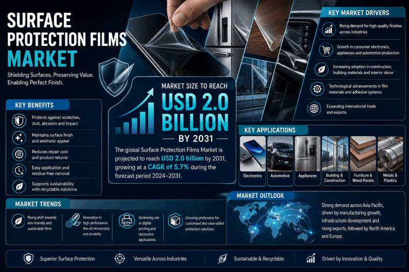
Surface Protection Films Market Size to Reach USD 2.0 Billion by 2031 as EV Disp …
According to DataM Intelligence, the surface protection films market is estimated at approximately USD 1.6 billion in 2026 and is expected to reach USD 2.0 billion by 2031, expanding at a 5.1% CAGR during 2024-2031. As manufacturing and logistics networks become more complex, protective films are increasingly being used as a cost-control and quality-assurance layer to preserve surface condition during processing, storage, transportation and delivery.
The role of protective…

Food Allergen Testing Market Size to Reach USD 2.48 Billion by 2035 as Label Acc …
According to DataM Intelligence, the food allergen testing market size is estimated at USD 1.35 billion in 2026 and is projected to reach USD 2.48 billion by 2035, expanding at a 6.96% CAGR from 2026 to 2035. As supply chains become more complex, allergen testing is moving beyond routine laboratory verification toward a strategic tool for recall prevention, supplier qualification, label assurance and brand-risk management. Food manufacturers are facing a…
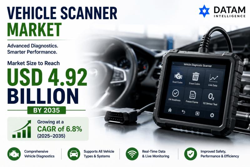
Vehicle Scanner Market Size to Reach USD 4.92 Billion by 2035, Driven by Border …
According to DataM Intelligence, the global vehicle scanner market size is estimated at approximately USD 2.79 billion in 2026 and is projected to reach USD 4.92 billion by 2035, expanding at a CAGR of 6.5% during 2026-2035. The market is being supported by increasing demand for non-intrusive vehicle inspection, stronger border-security requirements, rising screening needs across critical infrastructure, and growing adoption of high-throughput imaging, under-vehicle surveillance, automated image analysis, and…
More Releases for TSV
TSV Electroplating Additive Market Size, Growth Opportunities and Forecast 2025- …
Los Angeles, United State: A newly published report titled "Global TSV Electroplating Additive Market Insights, Forecast to 2025-2031" by QY Research throws light on the industry dynamics and current and future trends that play a key role in determining the business expansion. The global TSV Electroplating Additive market was valued at US$ 224 million in 2024 and is anticipated to reach US$ 372 million by 2031, witnessing a CAGR of…
Through Silicon Via (TSV) Technology Market 2022 | Detailed Report
The Through Silicon Via (TSV) Technology report compiles the market information depending upon market development and growth factors, optimizing the growth path. In addition, it highlights the strategies and market share of the leading vendors in the particular market. The report follows a robust research methodology model that helps to make informed decisions. It obtains both qualitative and quantitative market information supported by primary research.
The Through Silicon Via (TSV) Technology…
Through Silicon Via (TSV) Technology Market 2021 | Detailed Report
Global Through Silicon Via (TSV) Technology Market 2021-2027, has been prepared based on an in-depth market analysis with inputs from industry experts. The report covers the market landscape and its growth prospects in the coming years. The report includes a discussion of the key vendors operating in this market. An exclusive data offered in this report is collected by research and industry experts team.
Get Free Sample PDF (including full TOC,…
3D TSV and 2.5D Market Size, Share, Development by 2024
Market Research Report Store offers a latest published report on 3D TSV and 2.5D Market Analysis and Forecast 2019-2025 delivering key insights and providing a competitive advantage to clients through a detailed report.
The global 3D TSV and 2.5D market is valued at xx million USD in 2018 and is expected to reach xx million USD by the end of 2024, growing at a CAGR of xx% between 2019 and 2024.
The…
Global 3D TSV Market Share and Growth 2019 - QY Research
3D TSV is a vertical electrical connection (via) that passes completely through a silicon wafer or die. TSVs are high performance interconnect techniques used as an alternative to wire-bond and flip chips to create 3D packages and 3D integrated circuits. Compared to alternatives such as package-on-package, the interconnect and device density is substantially higher, and the length of the connections becomes shorter.
The global 3D TSV market is valued at xx…
3D TSV Packages Market Value Chain and Forecast 2016-2026
Currently, 3D Packaging using Through Silicon Via technology (3D TSV) is one of the hottest topics in the semiconductor ecosystem. 3D TSV is vertical electrical connection (via) passing completely through a silicon wafer or die. These short vertical interconnects are replacing the long interconnects of 2D packaging technologies including wire-bond and flip chips.
Growing demand for high density and multifunctional microelectronics with improved performance, and the reduction of timing delays is…

