Press release
Semiconductor Wafer Market to Reach US$ 35.3 Bn by 2033 from US$ 24.5 Bn at 5.4% CAGR

Semiconductor Wafer Market
Semiconductor Wafer Market Size and Trend Analysis
The global semiconductor wafer market is entering a transformative growth phase fueled by rising demand for advanced computing technologies, artificial intelligence (AI), electric vehicles (EVs), and next-generation telecommunications infrastructure. The market is projected to increase from US$ 24.5 billion in 2026 to US$ 35.3 billion by 2033, registering a CAGR of 5.4% during the forecast period. The market had already demonstrated solid momentum with a historical valuation of US$ 18.4 billion in 2020, reflecting resilient demand across multiple semiconductor applications and geographies. Semiconductor wafers serve as the foundational substrate for integrated circuits, logic chips, memory devices, sensors, and power semiconductors, making them indispensable to the modern electronics ecosystem. Increasing global investments in advanced semiconductor fabrication facilities, coupled with the rapid expansion of AI infrastructure and cloud computing, are accelerating the need for high-purity silicon and compound semiconductor wafers.
The Semiconductor Wafer Market is primarily driven by four structural forces: the global expansion of AI and high-performance computing workloads, accelerating automotive electrification, policy-led semiconductor localization initiatives, and the transition toward larger-diameter wafers for advanced-node fabrication. Asia Pacific dominates the market with a 66.5% share due to the strong concentration of semiconductor manufacturing hubs across Taiwan, China, South Korea, and Japan, while India is emerging as a strategic investment destination under the Semicon India Program. North America represents the fastest-growing regional market, supported by the U.S. CHIPS and Science Act and major domestic fabrication investments. The 300 mm wafer segment leads the market owing to its superior yield efficiency and scalability for advanced-node logic and memory fabrication, while compound semiconductor wafers such as silicon carbide (SiC) and gallium nitride (GaN) are witnessing rapid adoption due to the growing demand for EV power electronics, AI data centers, and 5G infrastructure.
Elevate your business strategy with comprehensive market data. Request a sample report now https://www.persistencemarketresearch.com/samples/36707
Key Highlights from the Report
✦ The global Semiconductor Wafer Market is expected to reach US$ 35.3 billion by 2033.
✦ Asia Pacific dominates the market with a 66.5% share due to concentrated semiconductor manufacturing capabilities.
✦ The 300 mm wafer segment holds the leading market share driven by advanced-node semiconductor fabrication demand.
✦ Compound semiconductor wafers including SiC and GaN are the fastest-growing material category globally.
✦ Logic devices account for the largest wafer consumption share due to rising AI processor demand.
✦ Government-backed semiconductor localization programs are accelerating global wafer fabrication investments.
Market Segmentation Analysis
The Semiconductor Wafer Market is segmented based on wafer size, material type, device type, and end-use applications. By wafer size, the market is categorized into 300 mm, 200 mm, and smaller-diameter wafers. Among these, 300 mm wafers dominate the market with approximately 68.5% share because they offer superior manufacturing efficiency, reduced cost-per-chip production, and higher yields for advanced-node semiconductor fabrication. Major manufacturers including GlobalWafers and Wafer Works are aggressively expanding 300 mm wafer capacity to support increasing demand from AI processors, GPUs, CPUs, and advanced memory devices. The rapid migration of semiconductor manufacturing toward sub-3nm process nodes further reinforces the importance of large-diameter wafers.
The 200 mm wafer segment is emerging as the fastest-growing category due to rising adoption of mature-node semiconductors, analog devices, industrial electronics, and power semiconductors. Silicon carbide and gallium nitride power devices used in EVs, renewable energy systems, and industrial automation are significantly increasing demand for 200 mm wafers. Despite short-term inventory corrections in some mature-node applications, the long-term outlook for this segment remains positive because of increasing investments in electrification and energy-efficient technologies.
By material type, the market is segmented into silicon wafers and compound semiconductor wafers. Silicon wafers dominate the industry with nearly 89% market share due to their widespread use across consumer electronics, automotive systems, industrial automation, and telecommunications devices. Polished silicon wafers account for the largest portion of the segment, while epitaxial wafers continue to gain traction in advanced power electronics and high-performance computing applications. Leading companies such as Shin-Etsu Chemical and SUMCO continue to maintain strong leadership in the global silicon wafer supply chain.
Compound semiconductor wafers, including SiC, GaN, and GaAs substrates, are experiencing the fastest growth rate due to the rapid expansion of EV charging infrastructure, AI servers, renewable energy systems, and 5G communications. These materials provide superior thermal conductivity, higher switching efficiency, and better power handling capabilities compared to traditional silicon, making them increasingly important in next-generation electronics.
Based on device type, the market includes logic devices, memory devices, analog ICs, sensors, and power semiconductors. Logic devices account for the largest market share because of the explosive growth in AI accelerators, advanced processors, and high-performance computing systems. Memory devices are also witnessing strong growth due to rising adoption of high-bandwidth memory (HBM) and AI-driven data center applications. Increasing demand for DRAM and NAND flash technologies continues to create significant opportunities for advanced wafer manufacturers.
Secure Your Full Report - Proceed to Checkout: https://www.persistencemarketresearch.com/checkout/36707
Market Drivers
One of the most significant drivers accelerating the Semiconductor Wafer Market is the global proliferation of artificial intelligence and advanced computing infrastructure. AI applications require massive computational power, driving unprecedented demand for high-performance GPUs, CPUs, and AI accelerators fabricated on advanced-node semiconductor wafers. The rapid expansion of hyperscale data centers and AI training clusters has substantially increased wafer consumption across logic and memory semiconductor segments. Semiconductor manufacturers are investing heavily in advanced fabrication technologies below the 3nm node, creating sustained demand for ultra-high-purity 300 mm wafers capable of supporting next-generation chip architectures.
Government-led semiconductor reindustrialization programs are another major growth catalyst for the industry. The United States, Europe, India, Japan, and several Southeast Asian nations are actively investing in domestic semiconductor manufacturing capacity to reduce reliance on concentrated Asian supply chains. The U.S. CHIPS and Science Act alone allocated more than US$ 52 billion toward semiconductor fabrication incentives and research initiatives, while the European Chips Act is mobilizing billions in public and private investments. India's Semicon India Program is also driving substantial investments in domestic wafer fabrication and compound semiconductor manufacturing facilities. These policy frameworks are strengthening long-term wafer procurement pipelines and encouraging large-scale greenfield manufacturing projects.
The accelerating electrification of automotive platforms is significantly boosting demand for compound semiconductor wafers. Modern EVs contain substantially higher semiconductor content compared to internal combustion vehicles, especially in power electronics systems such as traction inverters, onboard chargers, battery management systems, and fast-charging infrastructure. Silicon carbide and gallium nitride wafers are increasingly preferred for these applications because they offer higher efficiency, reduced energy losses, and improved thermal performance. As global EV adoption continues to rise, demand for wide-bandgap semiconductor wafers is expected to increase substantially.
The expansion of 5G infrastructure and advanced telecommunications networks is also supporting market growth. Telecom operators and equipment manufacturers require high-performance semiconductors for radio frequency components, edge computing infrastructure, and high-speed networking devices. Compound semiconductor wafers are particularly important for these applications due to their superior frequency handling capabilities and power efficiency.
Market Restraints
Despite favorable long-term growth prospects, the Semiconductor Wafer Market faces several operational and economic challenges. One of the primary restraints is the cyclical nature of semiconductor demand and inventory corrections. Wafer pricing often fluctuates based on downstream fab utilization rates, inventory levels, and macroeconomic conditions. Periods of oversupply can lead to pricing pressure and reduced profitability for wafer manufacturers. Inventory corrections in mature-node semiconductor applications have already impacted short-term demand for certain wafer categories, particularly 200 mm substrates.
High capital intensity represents another significant barrier within the industry. Semiconductor wafer manufacturing requires massive investments in ultra-clean fabrication environments, advanced crystal growth equipment, precision polishing technologies, and quality control systems. Building new wafer fabrication facilities often requires multi-billion-dollar investments, making market entry extremely challenging for new participants. Additionally, maintaining technological competitiveness demands continuous investment in R&D and process innovation.
Geopolitical tensions and supply chain concentration also pose risks to the global semiconductor ecosystem. A large portion of wafer manufacturing capacity remains concentrated in Asia Pacific, particularly in Taiwan, Japan, South Korea, and China. This concentration creates vulnerabilities related to trade restrictions, geopolitical instability, and logistics disruptions. Semiconductor manufacturers and governments are increasingly seeking geographic diversification strategies, but supply chain restructuring remains complex and capital intensive.
The rapid pace of technological change further increases operational challenges for wafer manufacturers. As semiconductor process nodes continue to shrink, wafer specifications become increasingly stringent, requiring exceptional levels of purity, flatness, and structural precision. Manufacturers unable to meet advanced-node quality requirements risk losing long-term supply agreements with leading semiconductor foundries.
Market Opportunities
The ongoing localization of semiconductor manufacturing in emerging economies presents one of the most significant growth opportunities for the Semiconductor Wafer Market. Governments across India, Southeast Asia, the Middle East, and North America are actively incentivizing domestic semiconductor production through subsidies, tax benefits, and infrastructure support programs. India's semiconductor ecosystem is evolving rapidly with projects such as Tata Electronics' silicon fab in Gujarat and new silicon carbide wafer facilities in Odisha. These initiatives create substantial greenfield opportunities for wafer suppliers seeking geographic diversification and long-term strategic partnerships.
The increasing adoption of compound semiconductor wafers across AI infrastructure, EVs, and renewable energy systems represents another major opportunity. Data center operators are seeking more energy-efficient power management systems to support escalating AI workloads, creating strong demand for SiC and GaN devices. Renewable energy infrastructure, including solar inverters and smart grids, also relies heavily on advanced power semiconductors. Wafer manufacturers capable of scaling cost-effective compound semiconductor production are expected to benefit significantly from this transition.
Advanced-node semiconductor fabrication continues to generate premium opportunities for high-precision wafer manufacturers. As leading chipmakers move toward 2nm and sub-2nm process technologies, the demand for ultra-high-quality wafers with exceptional purity and defect control is increasing rapidly. Manufacturers capable of consistently meeting these stringent specifications can command premium pricing and secure long-term supply agreements with advanced semiconductor foundries.
The rapid development of AI accelerators, high-bandwidth memory, and advanced packaging technologies is also creating new wafer demand patterns. Semiconductor companies are increasingly investing in heterogeneous integration, chiplet architectures, and advanced interconnect technologies that require highly specialized substrates and materials. This technological evolution is expected to create new growth avenues for innovative wafer suppliers.
Regional Insights
Asia Pacific dominates the global Semiconductor Wafer Market with a 66.5% share due to its unparalleled concentration of semiconductor manufacturing infrastructure and supply chain capabilities. Taiwan remains the global leader in advanced semiconductor fabrication, supported by TSMC's dominant foundry operations. South Korea and Japan continue to play critical roles through companies such as Samsung, SK Hynix, Shin-Etsu Chemical, and SUMCO. China's aggressive semiconductor expansion initiatives and rising domestic electronics demand are also strengthening regional market growth. India is emerging as a promising new entrant with increasing investments under the Semicon India Program and growing demand for domestic semiconductor production capabilities.
North America accounts for approximately 16% of the global market and is experiencing rapid growth due to semiconductor reindustrialization initiatives. The U.S. CHIPS and Science Act has triggered a wave of investments in domestic wafer fabrication and advanced semiconductor manufacturing. Projects such as GlobalWafers' Sherman, Texas facility and multiple advanced-node fabrication plants are expected to significantly strengthen domestic supply chain resilience over the coming decade. Rising demand for AI infrastructure and cloud computing further supports long-term wafer demand across the region.
Europe holds approximately 12.5% of the global Semiconductor Wafer Market, supported by strong materials science capabilities and established wafer manufacturers such as Siltronic AG and Soitec. The European Chips Act is accelerating investments in semiconductor R&D, advanced materials, and domestic fabrication capacity. Germany, France, Belgium, and the Netherlands continue to serve as major innovation centers for semiconductor technologies and advanced materials development.
Emerging regions including Southeast Asia and the Middle East are also attracting increasing semiconductor investments due to favorable government policies, rising electronics manufacturing activity, and strategic efforts to diversify global supply chains. These regions are expected to play a larger role in the future semiconductor manufacturing landscape.
Competitive Landscape and Company Insights
The global Semiconductor Wafer Market exhibits a highly consolidated oligopolistic structure dominated by a small group of major suppliers. Shin-Etsu Chemical, SUMCO Corporation, GlobalWafers, Siltronic AG, and SK Siltron collectively control a significant portion of the global silicon wafer supply. High capital requirements, long customer qualification cycles, and stringent quality standards create substantial barriers to entry, reinforcing the dominance of established players.
Competition within the market is increasingly centered around advanced-node capability development, compound semiconductor portfolio expansion, and geographic diversification strategies. Leading companies are investing heavily in larger-diameter wafers, ultra-high-purity substrate technologies, and AI-driven manufacturing optimization systems. Long-term supply agreements with leading semiconductor foundries remain a critical competitive advantage in the industry.
Company Insights
• Shin-Etsu Chemical Co., Ltd.
• SUMCO Corporation
• GlobalWafers Co., Ltd.
• Siltronic AG
• SK Siltron Co., Ltd.
• Wafer Works Corporation
• Okmetic
• LONGi Green Energy Technology Co., Ltd.
• Fujimi Incorporated
• SIEGERT WAFER GmbH
Recent industry developments highlight the market's strategic shift toward larger-diameter and advanced semiconductor wafers. In March 2024, Siltronic AG announced the discontinuation of small-diameter polished and epitaxial wafer production to focus on 200 mm and 300 mm wafer manufacturing. In June 2022, GlobalWafers initiated construction of a large-scale 300 mm wafer fabrication facility in Sherman, Texas, aimed at strengthening domestic U.S. semiconductor supply chains and supporting advanced-node chip manufacturing.
Reasons to Buy the Report
✔ Gain detailed analysis of market size, trends, and future growth opportunities through 2033.
✔ Understand the impact of AI, EV electrification, and semiconductor localization initiatives on wafer demand.
✔ Analyze competitive strategies, investment trends, and technological advancements among leading manufacturers.
✔ Access comprehensive regional insights covering Asia Pacific, North America, Europe, and emerging markets.
✔ Identify high-growth opportunities across compound semiconductor wafers, advanced-node fabrication, and power electronics applications.
Do You Have Any Query Or Specific Requirement? Request Customization of Report: https://www.persistencemarketresearch.com/request-customization/36707
Conclusion
The Semiconductor Wafer Market is positioned for sustained long-term growth driven by AI expansion, automotive electrification, cloud infrastructure development, and semiconductor supply chain localization efforts worldwide. Increasing investments in advanced semiconductor fabrication, coupled with rising demand for high-performance computing and power electronics, are transforming the competitive and technological landscape of the industry. Asia Pacific will continue to maintain its dominant position due to its concentrated manufacturing ecosystem, while North America and Europe accelerate domestic semiconductor reindustrialization initiatives. Compound semiconductor wafers such as silicon carbide and gallium nitride are expected to emerge as critical growth engines for the market as EVs, AI data centers, and renewable energy systems expand globally. As semiconductor technologies continue to evolve toward smaller process nodes and more complex architectures, wafer manufacturers capable of delivering advanced, high-purity substrates will remain central to the future of the global electronics industry.
Related Reports:
Video Surveillance Market https://www.persistencemarketresearch.com/market-research/video-surveillance-market.asp
Serverless Computing Market https://www.persistencemarketresearch.com/market-research/serverless-computing-market.asp
Secure Multiparty Computation (SMPC) Market https://www.persistencemarketresearch.com/market-research/secure-multiparty-computation-smpc-market.asp
Contact Us:
Persistence Market Research
Second Floor, 150 Fleet Street,
London, EC4A 2DQ, United Kingdom
USA Phone: +1 646-878-6329
UK Phone: +44 203-837-5656
Email: sales@persistencemarketresearch.com
Web: https://www.persistencemarketresearch.com
About Persistence Market Research:
At Persistence Market Research, we specialize in creating research studies that serve as strategic tools for driving business growth. Established as a proprietary firm in 2012, we have evolved into a registered company in England and Wales in 2023 under the name Persistence Research & Consultancy Services Ltd. With a solid foundation, we have completed over 3600 custom and syndicate market research projects, and delivered more than 2700 projects for other leading market research companies' clients.
Our approach combines traditional market research methods with modern tools to offer comprehensive research solutions. With a decade of experience, we pride ourselves on deriving actionable insights from data to help businesses stay ahead of the competition. Our client base spans multinational corporations, leading consulting firms, investment funds, and government departments. A significant portion of our sales comes from repeat clients, a testament to the value and trust we've built over the years.
This release was published on openPR.
Permanent link to this press release:
Copy
Please set a link in the press area of your homepage to this press release on openPR. openPR disclaims liability for any content contained in this release.
You can edit or delete your press release Semiconductor Wafer Market to Reach US$ 35.3 Bn by 2033 from US$ 24.5 Bn at 5.4% CAGR here
News-ID: 4530026 • Views: …
More Releases from Persistence Market Research
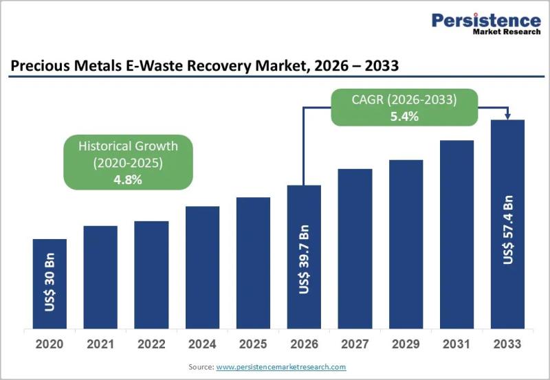
Precious Metals E-Waste Recovery Market to Reach US$ 57.4 Bn by 2033, Growing at …
The global precious metals e-waste recovery market is witnessing strong structural growth as rising electronic consumption, resource scarcity, and circular economy initiatives reshape global materials supply chains. The market is valued at US$ 39.7 Bn in 2026 and is projected to reach US$ 57.4 Bn by 2033, expanding at a CAGR of 5.4% during the forecast period. Increasing volumes of discarded electronics containing high-value metals such as gold, palladium, silver,…

Free Space Optics Market to Reach US$1.1 Billion by 2033, Growing at 15.8% CAGR …
The global Free Space Optics (FSO) market is emerging as a transformative segment within next-generation wireless communication, enabling ultra-high-speed optical data transmission through light propagation in free space. The market is projected to be valued at US$ 0.42 billion in 2026 and is expected to reach US$ 1.1 billion by 2033, growing at a strong CAGR of 15.8% during the forecast period. Growth is primarily driven by rising demand for…

Artificial Intelligence as a Service Market to Reach US$189.1 Bn by 2033 from US …
The global Artificial Intelligence as a Service (AIaaS) Market is experiencing exceptional growth as enterprises increasingly seek cost-effective and scalable ways to adopt artificial intelligence technologies without building expensive in-house infrastructure. The market is projected to expand from US$ 23.5 billion in 2026 to US$ 189.1 billion by 2033, registering a remarkable CAGR of 34.7% during the forecast period. AIaaS solutions are transforming how organizations deploy machine learning, predictive analytics,…
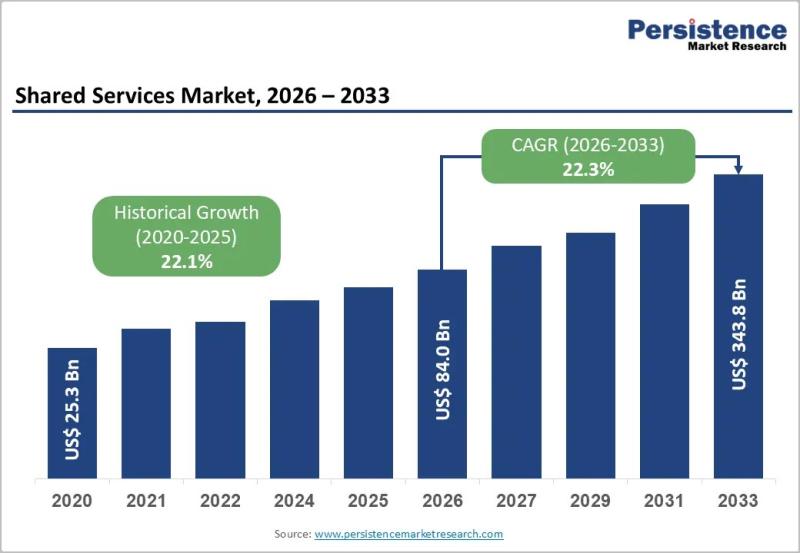
Shared Services Market to Reach US$343.8 Billion by 2033, Growing at a CAGR of 2 …
Shared Services Market Size, Share, Growth Trends, and Forecast Analysis 2026-2033
Shared Services Market Size and Trends Analysis
The global shared services market is undergoing a major transformation as enterprises increasingly centralize back-office functions to improve efficiency, reduce operational costs, and accelerate digital transformation initiatives. The market is projected to be valued at US$ 84.0 billion in 2026 and is expected to reach US$ 343.8 billion by 2033, registering a remarkable CAGR…
More Releases for Wafer
Wafer Surface Thinning Machine Market 2026-2032: Fully Automatic Wafer Grinders, …
Global Leading Market Research Publisher QYResearch announces the release of its latest report "Wafer Surface Thinning Machine - Global Market Share and Ranking, Overall Sales and Demand Forecast 2026-2032". For semiconductor fabs, OSATs (outsourced semiconductor assembly and test providers), and institutional investors tracking advanced packaging, the wafer back-grinding process has emerged as a critical bottleneck and differentiator. As 3D stacking, fan-out wafer-level packaging (FOWLP), and power device miniaturization intensify, the…
Semiconductor Silicon Wafer Market Is Going to Boom |• Silicon Wafer • Globa …
Worldwide Market Reports has released a new in-depth research study on the "Semiconductor Silicon Wafer Market," highlighting strong growth potential in the coming years. The report delivers a structured and data-driven analysis of the market landscape, combining robust research methodology, market sizing, validated data modeling, and insights sourced from reliable primary and secondary channels.
The study thoroughly examines key market aspects, including growth drivers, restraints, challenges, emerging opportunities, technological advancements, innovation…
Wafer Hybrid Bonding Equipment Market Share Driven by Wafer-to-Wafer Technology …
Wafer Hybrid Bonding Equipment Market Size
The global market for Wafer Hybrid Bonding Equipment was valued at US$ 164 million in the year 2024 and is projected to reach a revised size of US$ 756 million by 2031, growing at a CAGR of 24.7% during the forecast period.
View sample report
https://reports.valuates.com/request/sample/QYRE-Auto-31W14822/Global_Wafer_Hybrid_Bonding_Equipment_Market_Insights_Forecast_to_2029
The Wafer Hybrid Bonding Equipment market is experiencing accelerated growth, driven by increasing demand for advanced semiconductor packaging technologies that enable higher…
Semiconductor Wafer Electrostatic Chucks for 300mm Wafer Market
Semiconductor Wafer Electrostatic Chucks for 300mm Wafer Market
The global Semiconductor Wafer Electrostatic Chucks for 300mm Wafer market was valued at US$ 1165 million in 2023 and is anticipated to reach US$ 1672.7 million by 2030, witnessing a CAGR of 5.3% during the forecast period 2024-2030.
View Sample Report
https://reports.valuates.com/request/sample/QYRE-Auto-38F13137/Global_Semiconductor_Wafer_Electrostatic_Chucks_for_300mm_Wafer_Market_Research_Report_2023
Report Scope
The Semiconductor Wafer Electrostatic Chucks for 300mm Wafer market size, estimations, and forecasts are provided in terms of output/shipments (Units) and revenue…
Automatic Mounter Wafer Equipment Market Report 2018: Segmentation by Type (100 …
Global Automatic Mounter Wafer Equipment market research report provides company profile for Lintec Corporation, Nitto Denko, Tokyo Electron, Technovision, Takatori, Ultron Systems, DISCO Corp., Syagrus Systems, Advanced Dicing Technologies, Longhill Industries and Others.
This market study includes data about consumer perspective, comprehensive analysis, statistics, market share, company performances (Stocks), historical analysis 2012 to 2017, market forecast 2018 to 2025 in terms of volume, revenue, YOY growth rate, and CAGR for…
EMEA Solar Wafer Cutting Fluid PEG Market For Semiconductor, Solar Wafer, Crysta …
Latest industry research report on: EMEA (Europe, Middle East and Africa) Solar Wafer Cutting Fluid PEG Market : Industry Size, Share, Research, Reviews, Analysis, Strategies, Demand, Growth, Segmentation, Parameters, Forecasts
Request For Sample Report @ https://www.marketresearchreports.biz/sample/sample/1194694
Geographically, this report split EMEA into Europe, the Middle East and Africa, With sales (K MT), revenue (Million USD), market share and growth rate of Solar Wafer Cutting Fluid PEG for these regions, from 2012 to…
