Press release
Atomic Layer Deposition Market to Reach USD 6.87 Billion by 2033 as AI Chips, 2nm Logic, 3D Memory, and Advanced Materials Push Manufacturing Into the Angstrom Era
Atomic Layer Deposition Market
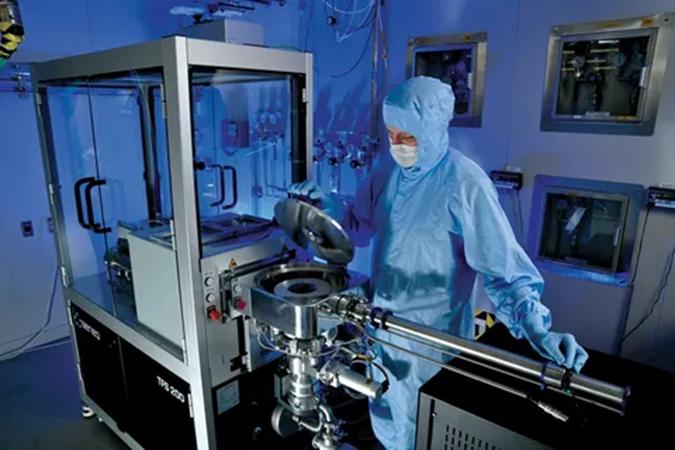
The global atomic layer deposition market is entering a decisive growth phase as semiconductor manufacturing moves deeper into atomic-scale engineering. The market is no longer being shaped only by demand for thinner films. It is being reshaped by the need to control materials at the level of individual atomic layers across advanced logic, high-bandwidth memory, 3D NAND, power devices, compound semiconductors, displays, solar cells, fuel cells, and medical devices.
Request Executive Sample | Market Intelligence: https://www.datamintelligence.com/download-sample/atomic-layer-deposition-market?kailas
Atomic layer deposition, widely known as ALD, enables ultra-thin film deposition with exceptional conformality, thickness control, and material uniformity. These characteristics are becoming essential as chipmakers move from planar structures to complex three-dimensional architectures. In advanced semiconductors, every additional layer, gate stack, barrier film, dielectric, metal fill, and interface material can influence performance, leakage, yield, and power efficiency.
The market's growth from USD 2.70 billion in 2025 to USD 6.87 billion by 2033 reflects a larger manufacturing transition. Chip production is entering a period where performance improvement is increasingly delivered by materials engineering rather than simple transistor scaling. Applied Materials describes ALD as a crucial enabler across advanced planar devices and the industry's transition to 3D architectures, with adoption also expanding across ICAPS applications such as passivation, encapsulation, and optical functions.
The major growth driver is the sharp rise in AI, high-performance computing, advanced memory, and foundry investments. SEMI reported that global semiconductor manufacturing equipment sales were forecast to reach a record USD 125.5 billion in 2025, supported by AI and leading-edge technology transitions. This matters for ALD because deposition intensity rises as devices become smaller, taller, denser, and more material-complex.
Recent Developments in the Atomic Layer Deposition Market
1. Lam Research launched a molybdenum ALD tool for advanced chip metallization.
In February 2025, Lam Research unveiled ALTUS Halo, described by the company as the world's first ALD tool using molybdenum for leading-edge semiconductor production. The system is designed for high-precision, low-resistivity, void-free molybdenum metallization, addressing the growing need for better feature fill in advanced chips. This is a major development because interconnect resistance and metal fill challenges are becoming more serious as device dimensions shrink.
2. ASM continues to position ALD as a core technology for next-generation devices.
ASM's 2025 annual report highlights the role of its deposition tools in enabling future semiconductor devices as AI and digital transformation continue to fuel advanced-node logic and memory capacity. ASM has historically been one of the most important ALD technology leaders, and its continued focus on deposition precision reinforces the market's shift toward atomic-scale manufacturing control.
3. Tokyo Electron is advancing high-productivity ALD for semiconductor manufacturing.
Tokyo Electron's NT333 series is the company's first semi-batch ALD chamber. The system uses spatial ALD to deliver atomic-level film thickness control, high film quality, and stronger productivity than conventional time-divided ALD methods. This is important because the market is not only asking for precision; it is asking for precision at production scale.
4. TSMC's 2nm transition is raising the importance of atomic-level deposition.
TSMC states that its 2nm technology started volume production in the fourth quarter of 2025 and features first-generation nanosheet transistor technology. Nanosheet and gate-all-around architectures require tighter film control around complex 3D structures, which strengthens the long-term demand case for ALD tools and processes.
5. Japan's Rapidus 2nm program is creating a strategic regional opportunity for ALD suppliers.
In April 2025, Rapidus announced that NEDO had approved its FY2025 plan and budget for 2nm-generation semiconductor integration technologies and chiplet-related manufacturing technology. Japan's 2nm ambitions are relevant for ALD because advanced-node process integration requires extreme control of gate stacks, spacers, barriers, liners, and dielectric layers.
Market Segmentation Analysis
The atomic layer deposition market is segmented by Type into Precursor Type, Material Type, Film Type, and Others. By Product, the market includes Aluminum Oxide, Plasma Enhanced, Catalytic, Metal, and Others. By Application, the market covers Solar Panels, Semiconductor, Flat Panel Display, Magnetic Heads, Fuel Cell, Medical Equipment, Research and Development, and Others. Regionally, the market covers North America, Latin America, Europe, Asia Pacific, the Middle East, and Africa.
By application, semiconductor is the dominant segment. The semiconductor segment is estimated to account for 61.0% of the global market in 2025, equal to USD 1.65 billion, and is projected to reach approximately USD 4.46 billion by 2033 if its share rises to 65.0%. This segment leads because ALD is deeply connected to the most valuable parts of semiconductor process integration. Advanced logic, DRAM, 3D NAND, high-bandwidth memory, image sensors, power semiconductors, and compound devices all require conformal films in increasingly difficult geometries. As chipmakers move toward nanosheet transistors, backside power delivery, 3D stacking, and advanced packaging, ALD becomes less optional and more foundational.
By product, plasma-enhanced ALD is one of the fastest-growing categories. Plasma-enhanced ALD is estimated to represent 28.0% of the market in 2025, equal to USD 756.00 million, and could reach USD 2.06 billion by 2033 at an estimated 30.0% share. PEALD is gaining attention because it can support lower-temperature processing, improved film density, and stronger control over reactive chemistries. This is valuable for sensitive substrates, advanced logic integration, displays, MEMS, and medical devices. The growing use of PEALD tools in research and advanced production environments shows that customers are seeking more flexible process windows rather than relying only on conventional thermal ALD.
By material and film opportunity, aluminum oxide remains a high-volume workhorse, while metal ALD is moving into premium growth. Aluminum oxide is widely used because it offers strong barrier, passivation, dielectric, and encapsulation properties across semiconductors, displays, solar cells, and protective coatings. However, metal ALD is becoming a higher-value growth area as chipmakers search for better materials for interconnects, liners, barriers, contacts, and advanced transistor structures. Lam Research's molybdenum ALD launch is a clear example of this shift from ALD as a dielectric-coating technology to ALD as a critical metallization enabler.
United States Market Analysis
The United States is one of the most strategically important markets for atomic layer deposition because of its semiconductor manufacturing revival, advanced R&D ecosystem, AI chip demand, and federal support for domestic chip production. The U.S. market is not only buying ALD systems for production. It is also using ALD in university labs, national research facilities, pilot lines, and early-stage process development for next-generation logic, memory, photonics, and quantum devices.
The most important U.S. trend is the movement from capacity expansion to materials-led process innovation. AI accelerators, advanced CPUs, GPUs, and high-bandwidth memory require higher performance with better energy efficiency. This is pushing equipment suppliers and chipmakers toward more precise deposition solutions. ALD is central to this shift because it can place films inside deep trenches, high-aspect-ratio structures, and 3D device features where traditional deposition methods struggle.
A second under-discussed U.S. trend is the rise of ALD in research-to-production pipelines. Albany NanoTech, for example, added a plasma-enhanced ALD machine produced by Oxford Instruments Plasma Technology to support atomic-scale chip research. The facility serves as an important bridge between research and commercial-scale semiconductor manufacturing, with relevance to companies such as GlobalFoundries, Intel, Samsung, and Micron.
The U.S. market is also being shaped by export controls and supply-chain localization. Equipment suppliers face restrictions in some overseas markets, while U.S. fabs and allied-country fabs are increasing investment in advanced manufacturing capacity. For ALD vendors, this creates a dual commercial reality: demand is rising because of AI and advanced nodes, but geographic access, compliance, and customer concentration are becoming more important in sales strategy.
Japan Market Analysis
Japan's atomic layer deposition market is gaining new relevance as the country rebuilds its advanced semiconductor ecosystem. Japan already has deep strengths in semiconductor materials, chemicals, precision equipment, metrology, and manufacturing discipline. The next opportunity is to connect those strengths to 2nm logic, chiplets, advanced packaging, power semiconductors, and specialty devices.
Rapidus is the most visible catalyst. The company's NEDO-approved FY2025 projects cover 2nm-generation semiconductor integration technologies and chiplet manufacturing technology based on Japan-U.S. collaboration. This is not only a foundry story. It is a materials and equipment story. Advanced-node manufacturing requires precise control of films at dimensions where small variations can hurt yield, reliability, and performance. ALD suppliers with strong local service, process engineering capability, and compatibility with Japanese materials ecosystems are likely to benefit.
Japan also has a strong opportunity in ALD for power devices and compound semiconductors. Silicon carbide, gallium nitride, sensors, MEMS, photonics, and automotive electronics all require high-quality thin films and surface passivation. Japanese manufacturers are likely to value ALD processes that improve reliability, reduce defects, and support long product lifecycles, especially in automotive, industrial, and energy applications.
Tokyo Electron's ALD capabilities are especially relevant in Japan's domestic ecosystem. Its NT333 semi-batch ALD chamber highlights the market's focus on combining film precision with productivity. For Japan, where high-volume manufacturing discipline and process reliability are critical, ALD tools that deliver both atomic-level control and throughput will be central to competitive positioning.
Competitive Landscape
The leading competitive set in the atomic layer deposition market includes ASM International, Applied Materials, Lam Research, Tokyo Electron, Veeco Instruments, Oxford Instruments, Beneq, Picosun, SENTECH Instruments, Kurt J. Lesker, CVD Equipment Corporation, Forge Nano, Arradiance, Aixtron, and other specialized deposition technology suppliers. The market is also influenced by precursor and materials suppliers because ALD performance depends heavily on precursor chemistry, process temperature, film purity, and compatibility with customer device architectures.
The strongest suppliers will be those that can offer not only equipment, but process recipes, precursor integration, metrology alignment, service support, and proven production repeatability. In advanced semiconductor fabs, ALD buying decisions are closely tied to yield, integration risk, and long-term node roadmaps. This favors vendors with deep customer collaboration and strong installed bases.
Purchase Corporate License | Market Intelligence: https://www.datamintelligence.com/buy-now-page?report=atomic-layer-deposition-market?kailas
Analyst Views
The atomic layer deposition market is becoming a direct beneficiary of the semiconductor industry's move into the angstrom era. As device structures become more vertical, more layered, and more material-sensitive, ALD is turning into one of the most important process technologies in the fab.
From 2026 to 2033, the strongest demand will come from advanced semiconductors, 3D memory, gate-all-around transistors, high-bandwidth memory, power electronics, displays, and research applications. Semiconductor demand will dominate revenue, but solar panels, medical devices, fuel cells, and advanced coatings will provide additional growth pockets.
The key message for buyers is clear: ALD is no longer a specialized thin-film tool used only for select applications. It is becoming a manufacturing requirement wherever atomic-scale control determines performance. The companies that can deliver conformality, throughput, process stability, and material innovation will capture the highest-value opportunities.
The analyst view is that ALD will remain one of the most defensible growth segments within semiconductor equipment and advanced materials processing. The market's expansion to USD 6.87 billion by 2033 will be led by customers that need precision not as a technical preference, but as a commercial necessity.
Contact:
Fabian
DataM Intelligence 4market Research LLP
6th Floor, M2 Tech Hub, DataM Intelligence 4market Research LLP, Lalitha Nagar, Habsiguda, Secunderabad, Hyderabad, Telangana 500039
USA: +1 877-441-4866
UK: +44 161-870-5507
Email: fabian@datamintelligence.com
About DataM Intelligence
DataM Intelligence is a renowned provider of market research, delivering deep insights through pricing analysis, market share breakdowns, and competitive intelligence. The company specializes in strategic reports that guide businesses in high-growth sectors such as nutraceuticals and AI-driven health innovations.
To find out more, visit https://www.datamintelligence.com/ or follow us on Twitter, LinkedIn and Facebook.
This release was published on openPR.
Permanent link to this press release:
Copy
Please set a link in the press area of your homepage to this press release on openPR. openPR disclaims liability for any content contained in this release.
You can edit or delete your press release Atomic Layer Deposition Market to Reach USD 6.87 Billion by 2033 as AI Chips, 2nm Logic, 3D Memory, and Advanced Materials Push Manufacturing Into the Angstrom Era here
News-ID: 4514098 • Views: …
More Releases from DataM intelligence 4 Market Research LLP

Polymers in Electric Vehicles Market to Reach USD 2,382.17 Billion by 2035 as EV …
Global Polymers in Electric Vehicle Market was valued at USD 27.7 billion in 2025 and is projected to reach USD 2,382.17 billion by 2035, expanding at a CAGR of 56.0% during 2026 to 2035
The global polymers in electric vehicles market is entering an aggressive growth phase as automakers redesign vehicles around batteries, software-defined electronics, high-voltage systems, thermal safety, and lightweight structures. The opportunity is no longer limited to replacing metal…

BIPV Glass Market to Reach USD 32.5 Billion by 2033 as Buildings Become Power-Ge …
Global BIPV (Building Integrated Photovoltaics) Glass Market reached USD 2.61 billion in 2025 and is estimated to reach USD 32.5 billion by 2033, growing at a CAGR of 37.4% during 2026 to 2033
The global BIPV glass market is entering a high-growth phase as the construction, solar, and real estate sectors converge around one urgent commercial question: how can buildings generate clean electricity without sacrificing architectural value, usable space, or building-envelope…
Phase Change Materials Market to Reach USD 1,639.71 Million by 2033 as Thermal S …
Global Phase Change Materials Market is projected to reach USD 1,639.71 million by 2033 from USD 729.76 million in 2025, growing at a CAGR of 17.6% during 2026 to 2033
The global phase change materials market is moving from a niche material-science category into a practical energy-management solution for buildings, pharmaceuticals, food logistics, electronics, and renewable energy systems. The market's next stage of growth will not be shaped only by the…
Advanced Metering Infrastructure Market to Reach USD 77.3 Billion by 2033 as Uti …
Global Advanced Metering Infrastructure Market reached USD 30.4 billion in 2025 and is expected to reach USD 77.3 billion by 2033, growing at a CAGR of 12.4% during 2026 to 2033
The advanced metering infrastructure market is moving into a new phase where utilities are no longer buying smart meters only to automate billing. They are using AMI as the front-end data layer for grid visibility, outage response, demand flexibility, distributed…
More Releases for ALD
Adrenoleukodystrophy (ALD) Market Opportunities in 2034
Market Overview
The Adrenoleukodystrophy (ALD) Market is growing steadily as improvements in newborn screening, genetic diagnostics, and awareness of rare neurodegenerative disorders lead to earlier detection and clinical intervention.
ALD is a genetically inherited X-linked disorder caused by mutations in the ABCD1 gene, leading to the toxic accumulation of very long-chain fatty acids (VLCFAs) in the brain, adrenal glands, and spinal cord. The condition manifests in multiple forms, including childhood cerebral…
Technological Advances Propel Growth In The Ald Equipment Market Industry Trends …
Stay ahead with our updated market reports featuring the latest on tariffs, trade flows, and supply chain transformations.
ALD Equipment Market Size Valuation Forecast: What Will the Market Be Worth by 2025?
There has been a significant expansion in the ALD equipment market size in the past few years. The market is predicted to rise from $3.41 billion in 2024 to $3.7 billion in 2025, indicating a compound annual growth rate (CAGR)…
Surge In Electronics And Semiconductor Sector Propels Ald Equipment Market: Key …
The ALD Equipment Market Report by The Business Research Company delivers a detailed market assessment, covering size projections from 2025 to 2034. This report explores crucial market trends, major drivers and market segmentation by [key segment categories].
What Is the Expected ALD Equipment Market Size During the Forecast Period?
The market size for ALD equipment has significantly expanded in the last few years, poised to rise from $3.41 billion in 2024 to…
Primary Catalyst Driving ALD Equipment Market Evolution in 2025: Surge In Electr …
What combination of drivers is leading to accelerated growth in the ald equipment market?
Anticipations of a surge in the electronics and semiconductor industry are set to boost the ALD equipment market. The realm of electronics includes firms that engineer, produce, and distribute devices such as radios, televisions, music systems, computers, semiconductors, transistors, integrated circuits, etc. ALD equipment finds its use in these industries to fabricate substrates for microelectronics and nanotechnology.…
Atomic Layer Deposition Market May See a Big Move|ALD Vacuum Technologies, ALD N …
A Latest intelligence report published by Pro Market Reports with title "Global Atomic Layer Deposition Market Outlook to 2032". A detailed study accumulated to offer Latest insights about acute features of the Atomic Layer Deposition market. This report provides a detailed overview of key factors in the Global Atomic Layer Deposition Market and factors such as driver, restraint, past and current trends, regulatory scenarios and technology development. Some of the…
