


Press release
Semiconductor Lithography and Etching Equipment Market to Reach USD 96.21 Billion by 2032, as High-NA EUV, Atomic-Scale Etch and AI Chip Fabs Redefine Wafer Manufacturing
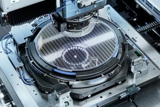
Semiconductor Lithography & Etching Equipment Market
Request For Exclusive Sample Report: https://www.globalreportsstore.com/request-sample/1381/
The report's headline number is important, but the deeper story is that lithography and etching are no longer separate equipment conversations. At advanced nodes, the pattern that lithography prints and the structure that etching transfers must be optimized together. AI accelerators, high-bandwidth memory, 3D NAND, gate-all-around transistors, chiplets and advanced packaging are forcing semiconductor manufacturers to think in terms of full process integration, not isolated tool purchases.
"Lithography and etching now sit at the center of semiconductor competitiveness," said a Global Reports Store spokesperson. "For CEOs, CTOs, VPs and product managers, the question is not only who can buy the next tool. The real question is who can control pattern fidelity, etch uniformity, defect density, overlay, throughput and cost per wafer at the same time. That is where the next manufacturing advantage will be created."
According to Global Reports Store, lithography equipment generated USD 29.76 billion in 2025, accounting for 53.70% of total market revenue, and is projected to reach USD 52.94 billion by 2032. Lithography remains the largest equipment category because EUV and High-NA EUV are becoming central to advanced logic, AI processors and future memory scaling. The report also notes that DUV systems continue to dominate volume deployments, accounting for more than 67% of lithography deployments in 2025, reflecting continued investment in mature-node production, automotive semiconductors, industrial chips and analog devices.
Etching equipment generated USD 25.67 billion in 2025, representing 46.30% of the market, and is projected to reach USD 43.27 billion by 2032. This segment is becoming more strategically important as device structures move deeper into 3D. FinFETs, gate-all-around structures, 3D NAND, DRAM scaling, advanced packaging and high-aspect-ratio features all require tighter etch control. The report identifies plasma etching, reactive ion etching and atomic layer etching as central technology areas, with atomic layer etching gaining traction where advanced-node precision is essential.
Application data shows the same advanced-computing pressure. Logic devices represented the largest application segment in 2025, generating USD 21.84 billion, driven by CPUs, GPUs and AI accelerators. Memory applications generated USD 18.72 billion, supported by DRAM, NAND and HBM scaling. Foundry services accounted for USD 9.63 billion, while advanced packaging contributed USD 5.24 billion and is emerging as a high-growth segment because chiplets and heterogeneous integration are increasing the value of patterning and etching beyond traditional front-end wafer fabrication.
Regionally, Asia-Pacific led the market with USD 33.18 billion in 2025, equal to 59.86% of global revenue, and is projected to reach USD 58.72 billion by 2032. The region's strength comes from the concentration of fabs in Taiwan, South Korea, China and Japan, as well as major government support for domestic semiconductor manufacturing. North America accounted for USD 10.47 billion in 2025, or 18.89% share, and is projected to reach USD 17.63 billion by 2032, supported by advanced semiconductor R&D, policy-backed fab investment and the presence of leading equipment and chip companies. Europe generated USD 8.96 billion, representing 16.16% share, and is forecast to reach USD 14.48 billion by 2032, with EUV lithography innovation remaining its strongest strategic position.
One under-discussed market shift is the rising cost of learning. High-NA EUV tools, advanced etchers and atomic-scale process modules are not simple capacity additions. They require years of process tuning, materials alignment, resist development, defect-control work, metrology integration and customer co-optimization. ASML's TWINSCAN EXE:5200B, for example, is a 0.55 NA High-NA EUV system designed to improve overlay and productivity versus the earlier EXE platform, while ASML's EUV product material describes High-NA systems as supporting 8 nm resolution and future advanced nodes starting at 2 nm logic.
This makes early ecosystem access extremely valuable. In March 2026, imec announced the arrival of ASML's EXE:5200 High-NA EUV system, calling it the most advanced lithography tool available and positioning it as a launchpad for the angstrom era. For the global market, this is not only a European R&D milestone. It is a signal that advanced chipmakers are already preparing the process recipes, materials and patterning flows that will shape future high-volume manufacturing.
The U.S. is also directly tied to this High-NA transition. Intel had already completed installation and begun calibration of the first commercial High-NA EUV lithography tool at its Oregon site, a 165-ton ASML system intended to support advanced process leadership. Intel's process material also identifies High-NA EUV as part of its future foundry roadmap for smaller process features.
Japan's role is different but highly strategic. Tokyo Electron is one of the most important suppliers in etch, coating, development, cleaning and adjacent wafer fabrication processes. In 2025, Tokyo Electron announced construction of a new production building in Miyagi with a construction cost of about JPY 104 billion, focused on semiconductor manufacturing equipment including plasma etch systems. TEL also completed a new development building in Miyagi, noting that increasing semiconductor complexity, finer chip line widths and evolving patterning technologies are expected to expand the market for etch systems developed and manufactured by Tokyo Electron Miyagi.
This is especially important because Japan is rebuilding its advanced semiconductor manufacturing base. Rapidus has stated that production of 2 nm semiconductors involves film deposition, lithography, etching and polishing, and that its IIM-1 foundry installed more than 200 pieces of equipment in roughly two and a half months before beginning lot operations in April 2025. Rapidus has also described EUV lithography as a key technology for realizing 2 nm semiconductors and said it was the first company to install advanced EUV machinery in Japan.
The U.S. etching and materials-engineering side is also gaining urgency. Applied Materials introduced two systems in April 2026 for angstrom-era logic chips, designed to create extremely small features in advanced 3D gate-all-around transistors. The company said the systems are being used by leading foundry-logic manufacturers at 2 nm and beyond, showing how materials engineering and atomic-level process control are becoming inseparable from advanced-node scaling.
Lam Research has similarly emphasized that deposition and etch intensity is rising as semiconductors shift to 3D architectures across NAND, DRAM, logic and advanced packaging. The company describes higher aspect ratios, perpendicular processing and EUV as forces reshaping chipmaking for the AI era. This reinforces Global Reports Store's view that etching equipment will not be a secondary category behind lithography. It will be one of the main bottleneck-solving layers for AI-era wafer fabrication.
For executives, the commercial model is changing. In older semiconductor cycles, equipment purchases were often discussed in terms of capacity expansion. In the current cycle, buyers are purchasing process capability, ecosystem access and manufacturing risk reduction. A fab does not simply need an EUV scanner or a plasma etcher. It needs a qualified flow that links resist, mask, lithography, etch, clean, metrology and defect inspection into a repeatable manufacturing system.
The winning manufacturers will be those that understand where bottlenecks are shifting: High-NA EUV availability, etch selectivity, high-aspect-ratio structure control, advanced packaging lithography, HBM-related process intensity, tool uptime, service support and yield learning speed. Equipment suppliers that can provide co-development, software-enabled process control, chamber matching, recipe transfer and global service capacity will have stronger negotiating power than suppliers selling stand-alone hardware.
Purchase This Exclusive Report: https://www.globalreportsstore.com/checkout/1381/
Key Developments
1. ASML reported strong 2026 demand signals for lithography systems. In April 2026, ASML reported EUR 8.8 billion in first-quarter net sales, 53.0% gross margin and EUR 2.8 billion in net income, while raising its 2026 net sales outlook to EUR 36 billion to EUR 40 billion. The figures support the view that lithography investment remains strong despite cost and geopolitical pressure.
2. Imec received ASML's EXE:5200 High-NA EUV system. In March 2026, imec announced the arrival of the advanced High-NA EUV tool, positioning it as a launchpad for angstrom-era process development. This matters for U.S. and Japanese customers because early process learning at imec influences the global adoption path for future nodes.
3. Tokyo Electron expanded Japan's etching infrastructure in Miyagi. TEL's Miyagi investment includes a new production building costing about JPY 104 billion for semiconductor production equipment including plasma etch systems, while its completed development building supports advanced patterning and etch technology needs.
4. Applied Materials introduced angstrom-era systems for 2 nm and beyond. In April 2026, Applied Materials launched new deposition systems for advanced 3D gate-all-around logic chips, with leading foundry-logic manufacturers using the technologies at 2 nm and beyond. This highlights the move from lithography-only scaling toward atomic-level materials engineering.
5. Rapidus advanced Japan's 2 nm manufacturing ecosystem. Rapidus reported that its IIM-1 foundry installed more than 200 pieces of equipment and began lot operations in April 2025, while also identifying EUV lithography as critical for 2 nm GAA manufacturing. This strengthens long-term Japanese demand for lithography, etching, deposition, polishing and metrology tools.
Global Reports Store believes the semiconductor lithography and etching equipment market is entering a high-complexity growth phase. The strongest opportunities will not come from broad fab expansion alone. They will come from equipment and process platforms that solve the hardest manufacturing problems: High-NA EUV readiness, advanced etch precision, 3D device scaling, HBM process intensity, chiplet packaging and yield control at atomic dimensions. For Japan and the United States, the market is becoming a test of who can turn capital investment into stable, high-yield advanced manufacturing.
Media Contact
Global Reports Store
Office No. 301, Sairam IT Park, Hadapsar, Pune 411028
Email: sales@globalreportsstore.com
Phone: +91 8143002442
About Global Reports Store
Global Reports Store provides market intelligence designed for strategic decision makers across technology, energy, industrial, automotive and emerging-growth sectors. Its research supports leadership teams with data-driven analysis, competitive mapping, segmentation insight and country-level market interpretation for investment, product planning and partnership decisions.
This release was published on openPR.
Permanent link to this press release:
Copy
Please set a link in the press area of your homepage to this press release on openPR. openPR disclaims liability for any content contained in this release.
You can edit or delete your press release Semiconductor Lithography and Etching Equipment Market to Reach USD 96.21 Billion by 2032, as High-NA EUV, Atomic-Scale Etch and AI Chip Fabs Redefine Wafer Manufacturing here
News-ID: 4512829 • Views: …
More Releases from Global Reports Store
Hydrochloric Acid Electrolysis Technology Market to Reach US$ 1,684.7 Million by …
Global Reports Store's research report titled Hydrochloric Acid Electrolysis Technology Market Report 2032, Report ID 2028, 265 pages, published in May 2026 and authored by Alex. According to the report, the global Hydrochloric Acid Electrolysis Technology Market was valued at US$ 842.5 million in 2025 and is projected to reach US$ 1,684.7 million by 2032, growing at a CAGR of 10.4% from 2026 to 2032. The market is segmented by…

Anhydrous Hydrofluoric Acid for Fluorochemicals Market to Reach US$ 3,360 Millio …
Global Reports Store's research report titled Anhydrous Hydrofluoric Acid for Fluorochemicals Market Strategic Outlook 2032, Report ID 2026, 245 pages, published in May 2026 and authored by Alex. According to the report, the global Anhydrous Hydrofluoric Acid for Fluorochemicals Market was valued at US$ 2,080 million in 2025 and is projected to reach US$ 3,360 million by 2032, expanding at a CAGR of 7.1% from 2026 to 2032.
The Anhydrous Hydrofluoric…

Semiconductor-Grade Hydrofluoric Acid Market to Reach US$ 4,046.8 Million by 203 …
Global Reports Store's research report titled Semiconductor-Grade Hydrofluoric Acid Market Report 2032, Report ID 2024, 230 pages, published in May 2026 and authored by Alex. According to the report, the global Semiconductor-Grade Hydrofluoric Acid Market was valued at US$ 2,108.4 million in 2025 and is projected to reach US$ 4,046.8 million by 2032, expanding at a CAGR of 9.8% from 2026 to 2032.
The Semiconductor-Grade Hydrofluoric Acid Market is entering a…
High-Purity Potassium Fluoride Market to Reach US$ 340 Million by 2032 as Semico …
Global Reports Store's research report titled High-Purity Potassium Fluoride Market Growth Report 2032, Report ID 2021, authored by Global Reports Store. According to the report, the global High-Purity Potassium Fluoride Market was valued at US$ 185 million in 2025 and is projected to reach US$ 340 million by 2032, expanding at a CAGR of 9.1% from 2026 to 2032. The report defines the market across anhydrous high-purity potassium fluoride, ultra-high-purity…
More Releases for EUV
Future of EUV Lithography Market (2035) | High-NA EUV, Semiconductor Manufacturi …
Extreme Ultraviolet Lithography (EUV) Market is valued at US$ 14.22 billion in 2025 and is projected to reach US$ 41.97 billion by 2035, growing at a CAGR of 11.4% during 2026-2035.
DataM Intelligence has released its latest "EUV Lithography Market Size 2026" report, delivering comprehensive insights into market trends, growth opportunities, competitive dynamics, and regional performance. The report covers market size by value and volume, CAGR forecasts, and emerging opportunities, the…
EUV Pellicle Market Size, Trends & Forecasts | Valuates Reports
EUV Pellicle Market Size
The global market for EUV Pellicle was valued at US$ 78.8 million in the year 2024 and is projected to reach a revised size of US$ 171 million by 2031, growing at a CAGR of 8.6% during the forecast period.
Get Free Sample: https://reports.valuates.com/request/sample/QYRE-Auto-17Z11340/Global_EUV_Pellicle_Market_Research_Report_2022?utm_source=prnewswire&utm_medium=referral
In a typical semiconductor process, a thin protective film is usually placed on the surface of the photomask to protect it from contaminants. This thin…
Extreme Ultraviolet (EUV) Lithography Market
Extreme Ultraviolet (EUV) Lithography Market Overview
Extreme ultraviolet lithography is an advanced version of lithography which uses an extreme ultra violet light of the shortest wavelength of 13.5 nm. Lithography is mainly used to print complicated patterns which are mostly highlight integrated circuits onto semiconductor wafers.
This report provides a deep insight into the global Extreme Ultraviolet (EUV) Lithography market covering all its essential aspects. This ranges from a macro overview of…
EUV Photoresists Market Revenue, Insights, Overview, Outlook, Analysis
EUV Photoresists Market Size
The global EUV Photoresists market is projected to grow from US$ 226.4 million in 2024 to US$ 878.9 million by 2030, at a Compound Annual Growth Rate (CAGR) of 25.4% during the forecast period.
Get Free Sample: https://reports.valuates.com/request/sample/QYRE-Auto-36H8625/Global_EUV_Photoresists_Market_Insights_Forecast_to_2028
Global key players of EUV Photoresists include TOK, JSR and Shin-Etsu Chemical, etc. The top three players hold a share over 90%. Japan is the largest market, has a share about…
EUV Lithography Market 2023 Size, Share, Growth Report 2030
Latest Updated Report 2023, The Global EUV Lithography Market to Growing A CAGR of % during forecast period of 2023-2030. The Market is segmented by Global EUV Lithography Market Breakdown by Application (Integrated Device Manufacturers (IDM), Foundry, Others) by Type (Light Source, Exposure Device, EUV Pod, Others) and by Geography (North America, South America, Europe, Asia Pacific, MEA).
The EUV Lithography Market 2023 Report makes available the current and forthcoming technical…
Greatest Progress in EUV Lithography (EUVL) Market, 2021-2026
(Portland, United States): Big Market Research newly added a research report on the EUV Lithography (EUVL) Market which represents a study for the period from 2021 to 2026. The research study provides a near look at the market scenario and dynamics impacting its growth. This report highlights the crucial developments along with other events happening in the market which are marking on the growth and opening doors for future growth…

