Press release
Semiconductor Wafer Market to Reach USD 40.4 Billion by 2036, Driven by AI Chip Boom and 300mm Capacity Expansion
Semiconductor Wafer Market
This expansion is being driven by a powerful convergence of factors-AI accelerator demand, aggressive foundry CAPEX cycles, and global semiconductor reshoring initiatives. As leading chipmakers ramp up investments in advanced nodes, semiconductor wafers-particularly 300mm-are becoming the critical foundation enabling next-generation computing performance.
Get detailed market forecasts, competitive benchmarking, and pricing trends:
https://www.futuremarketinsights.com/reports/sample/rep-gb-12824
Featured Snippet: Key Market Answer
Q: What is driving the growth of the semiconductor wafer market?
A: Growth is driven by rising AI chip demand, large-scale foundry capital expenditure (CAPEX), the transition from 200mm to 300mm wafers, and global semiconductor reshoring initiatives supported by government policies like the CHIPS Act and India's ISM 2.0.
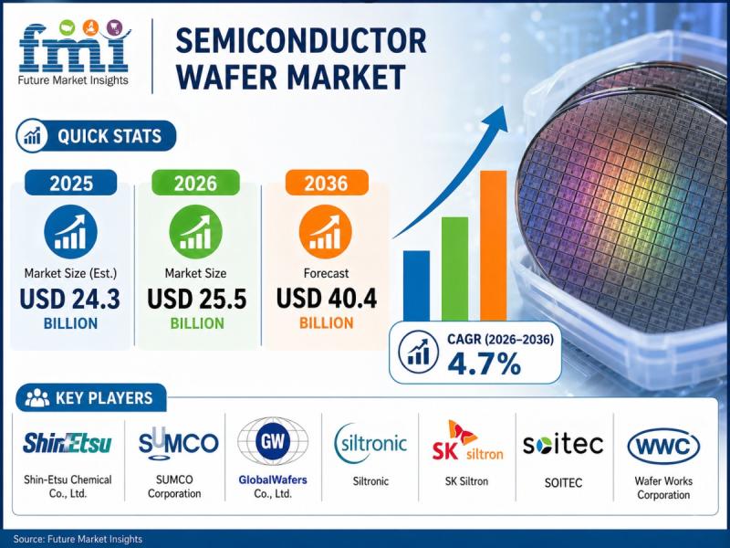
Quick Stats
Market Size (2025): ~USD 24.3 billion (est.)
Market Size (2026): USD 25.5 billion
Forecast (2036): USD 40.4 billion
CAGR (2026-2036): 4.7%
Incremental Opportunity: USD 14.9 billion
Leading Wafer Type: 300mm Silicon Wafers
Top Application Segment: Consumer Electronics
Dominant Process Node: 3nm (15.6% share in 2026)
Market Overview: Transition to AI-Driven Wafer Ecosystem
The semiconductor wafer market forms the backbone of the global electronics industry, supplying substrate materials essential for integrated circuit fabrication. The market is undergoing a structural shift toward:
• 300mm wafer dominance for advanced nodes
• AI and high-performance computing (HPC) applications
• Regionalized semiconductor supply chains
This transformation is underpinned by record-breaking foundry investments. Major players are aggressively expanding capacity to support AI-driven workloads, data centers, and next-gen consumer electronics.
Key Growth Drivers
1. AI Accelerator Demand Driving Foundry CAPEX
The explosive growth of AI workloads is pushing semiconductor manufacturers to expand fabrication capacity at an unprecedented scale. This directly increases demand for high-quality wafers used in advanced nodes (3nm and below).
2. Transition from 200mm to 300mm Wafers
Wafer manufacturers are phasing out legacy 200mm production in favor of 300mm wafers, which offer:
• Higher chip yield per wafer
• Lower cost per chip
• Better compatibility with advanced nodes
This shift is redefining supply dynamics and profitability across the industry.
3. Global Semiconductor Reshoring Initiatives
Government-backed programs are reshaping supply chains:
• US CHIPS Act
• EU Chips Act
• India's ISM 2.0
• Japan's METI subsidies
These initiatives are creating parallel semiconductor ecosystems, each requiring localized wafer production capacity.
Market Trends Shaping the Industry
• 300mm Capacity Expansion: Rapid investments in advanced wafer fabs globally
• Rise of Compound Semiconductors: Increasing use of SiC and GaN in EVs and power electronics
• AI Integration in Manufacturing: AI-driven metrology and predictive analytics optimizing wafer production
• Advanced Node Evolution: Growing adoption of 3nm and sub-2nm technologies
• Supply Chain Regionalization: Localization of wafer supply to reduce geopolitical risk
Segment Insights
Product Leadership: 300mm Silicon Wafers
300mm wafers dominate due to:
• High efficiency in advanced chip production
• Strong demand from AI, HPC, and data centers
• Superior economies of scale
Application Leadership: Consumer Electronics
The consumer electronics segment leads demand, driven by:
• Smartphones, laptops, and smart devices
• Increasing need for energy-efficient and high-performance chips
• Continuous innovation and device miniaturization
Process Node Dominance: 3nm (15.6%)
3nm wafers are gaining traction due to:
• Higher transistor density
• Improved power efficiency
• Strong adoption in AI chips and premium devices
Speak to Analyst: Customize insights for your business strategy:
https://www.futuremarketinsights.com/customization-available/rep-gb-12824
Regional Insights
Top Growth Markets (CAGR 2026-2036)
• India: 7.6% - Fastest growth driven by semiconductor policy push (ISM 2.0)
• UK: 5.2% - Growth supported by advanced R&D ecosystem
• China: 4.6% - Strong domestic innovation and smart factory expansion
• Germany: 4.4% - Industrial automation and automotive semiconductor demand
• USA: 4.3% - Consumer electronics demand and CHIPS Act investments
Global Leadership Landscape
• Japan: Dominates wafer production with over 50% share in 300mm capacity
• USA: Emerging as a key hub for advanced wafer manufacturing
• Asia-Pacific: Leads in volume consumption and manufacturing expansion
Competitive Landscape
The semiconductor wafer market is highly consolidated, with Tier 1 players controlling over 30% of global capacity. Competition is increasingly centered on:
• Advanced wafer technology
• Production scalability
• Supply chain localization
• R&D investment
Key Players
• Shin-Etsu Chemical Co., Ltd.
• SUMCO Corporation
• GlobalWafers Co., Ltd.
• Siltronic
• SK Siltron
• SOITEC
• Wafer Works Corporation
Competitive Differentiation Factors
• Advanced node compatibility (3nm and below)
• Wafer size innovation (300mm scaling)
• Material specialization (SiC, GaN)
• Strategic fab partnerships and long-term supply contracts
Recent Developments
• Major foundries significantly increased capital expenditure for AI chip production
• Expansion of 300mm wafer manufacturing facilities in the USA
• Strategic exit from 200mm wafer production by leading suppliers
• Growth in compound semiconductor wafer production (SiC & GaN)
• Government-backed semiconductor ecosystem development across key regions
Expert Insight
The semiconductor wafer market is entering a capacity-constrained growth phase, where the pace of wafer supply expansion will directly influence global AI chip production.
Manufacturers that align investments with advanced node demand, regional supply chain shifts, and next-generation materials will capture disproportionate market share in the coming decade.
FAQs
1. What is the future outlook for the semiconductor wafer market?
The market is projected to reach USD 40.4 billion by 2036, growing at a CAGR of 4.7%, driven by AI demand and semiconductor manufacturing expansion.
2. Which wafer type dominates the market?
300mm silicon wafers dominate due to their efficiency and compatibility with advanced semiconductor nodes.
3. Why is the transition from 200mm to 300mm important?
300mm wafers enable higher chip output, lower production costs, and better support for advanced technologies like AI and HPC.
4. What are the key challenges in the market?
• High capital investment requirements
• Supply chain disruptions
• Geopolitical tensions
• Transition complexity from legacy systems
5. Which regions offer the highest growth potential?
India leads growth, while China and the USA remain key contributors to global demand and innovation.
Unlock 360° insights for strategic decision making and investment planning:
https://www.futuremarketinsights.com/reports/semiconductor-wafers-market
Conclusion
The semiconductor wafer market sits at the core of the digital economy, enabling advancements in AI, cloud computing, automotive electronics, and next-generation consumer devices.
As the industry transitions toward AI-driven computing, advanced nodes, and regionalized supply chains, semiconductor wafers will become even more strategically critical.
With strong investment momentum and evolving technological frontiers, the market is set to play a defining role in shaping the future of global semiconductor innovation.
Browse More Related Reports!
Power Management System Market - https://www.futuremarketinsights.com/reports/power-management-system-market
3D Camera Market - https://www.futuremarketinsights.com/reports/3d-camera-market
E-passport Market - https://www.futuremarketinsights.com/reports/epassport-market
Contact Us:
Future Market Insights Inc.
Christiana Corporate, 200 Continental Drive,
Suite 401, Newark, Delaware - 19713, USA
T: +1-347-918-3531
For Sales Enquiries: sales@futuremarketinsights.com
About Future Market Insights (FMI)
Future Market Insights, Inc. (FMI) is an ESOMAR-certified, ISO 9001:2015 market research and consulting organization, trusted by Fortune 500 clients and global enterprises. With operations in the U.S., UK, India, and Dubai, FMI provides data-backed insights and strategic intelligence across 30+ industries and 1200 markets worldwide.
This release was published on openPR.
Permanent link to this press release:
Copy
Please set a link in the press area of your homepage to this press release on openPR. openPR disclaims liability for any content contained in this release.
You can edit or delete your press release Semiconductor Wafer Market to Reach USD 40.4 Billion by 2036, Driven by AI Chip Boom and 300mm Capacity Expansion here
News-ID: 4490199 • Views: …
More Releases from Future Market Insights
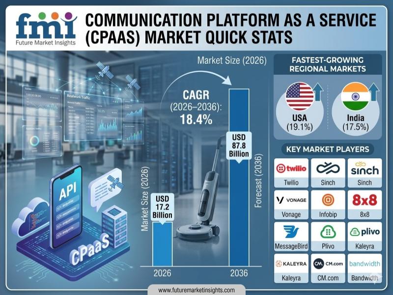
Communication Platform as a Service (CPaaS) Market to Surpass USD 87.8 Billion b …
The global Communication Platform as a Service (CPaaS) market is entering a hyper-growth phase as enterprises accelerate the integration of voice, messaging, and video into digital applications and customer engagement workflows. Valued at USD 17.2 billion in 2026, the market is projected to reach USD 87.8 billion by 2036, expanding at a robust CAGR of 18.4%.
This growth represents an incremental opportunity of USD 70.6 billion, fueled by enterprise demand for…
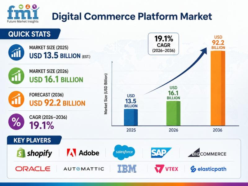
Digital Commerce Platform Market to Reach USD 92.2 Billion by 2036, Driven by AI …
The global digital commerce platform market is entering a hyper-growth phase as enterprises transition from channel-centric ecommerce architectures to platform-centric operating models. According to the latest analysis, the market is valued at USD 16.1 billion in 2026 and is projected to reach USD 92.2 billion by 2036, expanding at a CAGR of 19.1%. The sector is expected to generate an incremental opportunity of USD 76.1 billion over the forecast period.
This…
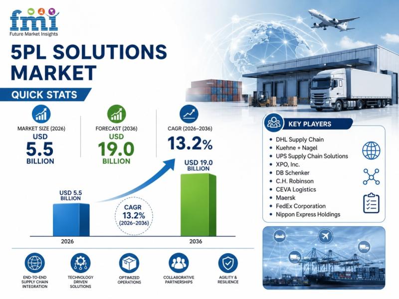
5PL Solutions Market to Reach USD 19.0 Billion by 2036, Driven by AI-Led Orchest …
The global 5PL solutions market is entering a rapid expansion phase as supply chains evolve from fragmented execution models to unified, intelligence-driven orchestration systems. According to the latest analysis, the market is valued at USD 5.5 billion in 2026 and is projected to reach USD 19.0 billion by 2036, expanding at a CAGR of 13.2%. The sector is expected to generate an incremental opportunity of USD 13.5 billion over the…
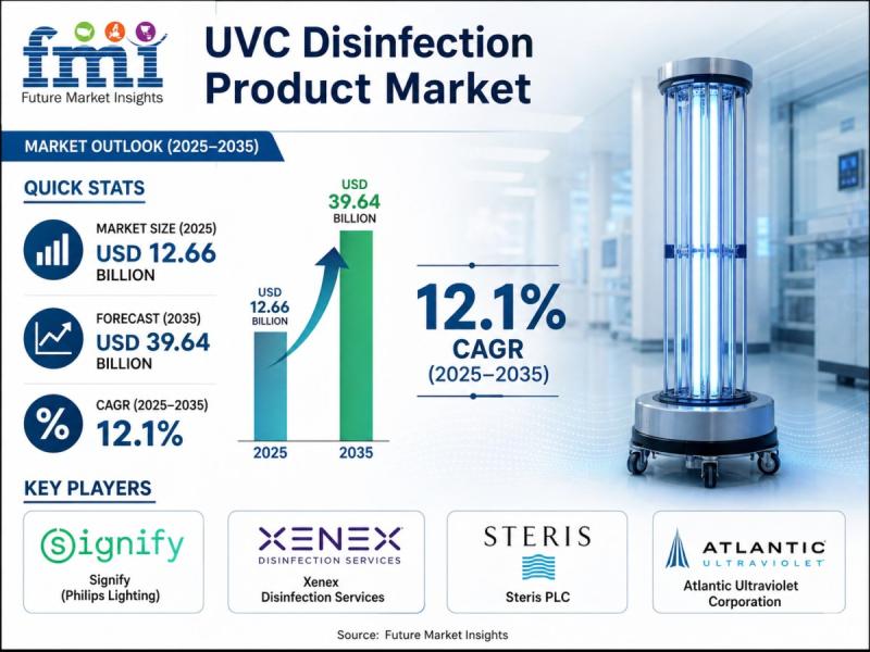
UVC Disinfection Product Market to Reach USD 39.64 Billion by 2035, Driven by In …
The global UVC disinfection product market is entering a rapid expansion phase as hygiene, infection control, and public health safety become top global priorities. The market is valued at USD 12.66 billion in 2025 and is projected to reach USD 39.64 billion by 2035, growing at a CAGR of 12.1% over the forecast period. The industry is expected to generate an incremental opportunity of USD 26.98 billion.
This growth reflects a…
More Releases for Wafer
Wafer Surface Thinning Machine Market 2026-2032: Fully Automatic Wafer Grinders, …
Global Leading Market Research Publisher QYResearch announces the release of its latest report "Wafer Surface Thinning Machine - Global Market Share and Ranking, Overall Sales and Demand Forecast 2026-2032". For semiconductor fabs, OSATs (outsourced semiconductor assembly and test providers), and institutional investors tracking advanced packaging, the wafer back-grinding process has emerged as a critical bottleneck and differentiator. As 3D stacking, fan-out wafer-level packaging (FOWLP), and power device miniaturization intensify, the…
Semiconductor Silicon Wafer Market Is Going to Boom |• Silicon Wafer • Globa …
Worldwide Market Reports has released a new in-depth research study on the "Semiconductor Silicon Wafer Market," highlighting strong growth potential in the coming years. The report delivers a structured and data-driven analysis of the market landscape, combining robust research methodology, market sizing, validated data modeling, and insights sourced from reliable primary and secondary channels.
The study thoroughly examines key market aspects, including growth drivers, restraints, challenges, emerging opportunities, technological advancements, innovation…
Wafer Hybrid Bonding Equipment Market Share Driven by Wafer-to-Wafer Technology …
Wafer Hybrid Bonding Equipment Market Size
The global market for Wafer Hybrid Bonding Equipment was valued at US$ 164 million in the year 2024 and is projected to reach a revised size of US$ 756 million by 2031, growing at a CAGR of 24.7% during the forecast period.
View sample report
https://reports.valuates.com/request/sample/QYRE-Auto-31W14822/Global_Wafer_Hybrid_Bonding_Equipment_Market_Insights_Forecast_to_2029
The Wafer Hybrid Bonding Equipment market is experiencing accelerated growth, driven by increasing demand for advanced semiconductor packaging technologies that enable higher…
Semiconductor Wafer Electrostatic Chucks for 300mm Wafer Market
Semiconductor Wafer Electrostatic Chucks for 300mm Wafer Market
The global Semiconductor Wafer Electrostatic Chucks for 300mm Wafer market was valued at US$ 1165 million in 2023 and is anticipated to reach US$ 1672.7 million by 2030, witnessing a CAGR of 5.3% during the forecast period 2024-2030.
View Sample Report
https://reports.valuates.com/request/sample/QYRE-Auto-38F13137/Global_Semiconductor_Wafer_Electrostatic_Chucks_for_300mm_Wafer_Market_Research_Report_2023
Report Scope
The Semiconductor Wafer Electrostatic Chucks for 300mm Wafer market size, estimations, and forecasts are provided in terms of output/shipments (Units) and revenue…
Automatic Mounter Wafer Equipment Market Report 2018: Segmentation by Type (100 …
Global Automatic Mounter Wafer Equipment market research report provides company profile for Lintec Corporation, Nitto Denko, Tokyo Electron, Technovision, Takatori, Ultron Systems, DISCO Corp., Syagrus Systems, Advanced Dicing Technologies, Longhill Industries and Others.
This market study includes data about consumer perspective, comprehensive analysis, statistics, market share, company performances (Stocks), historical analysis 2012 to 2017, market forecast 2018 to 2025 in terms of volume, revenue, YOY growth rate, and CAGR for…
EMEA Solar Wafer Cutting Fluid PEG Market For Semiconductor, Solar Wafer, Crysta …
Latest industry research report on: EMEA (Europe, Middle East and Africa) Solar Wafer Cutting Fluid PEG Market : Industry Size, Share, Research, Reviews, Analysis, Strategies, Demand, Growth, Segmentation, Parameters, Forecasts
Request For Sample Report @ https://www.marketresearchreports.biz/sample/sample/1194694
Geographically, this report split EMEA into Europe, the Middle East and Africa, With sales (K MT), revenue (Million USD), market share and growth rate of Solar Wafer Cutting Fluid PEG for these regions, from 2012 to…
