Press release
NANOSENSORS™ introduces AdvancedTEC AFM Probes with Gold and Platinum Coating
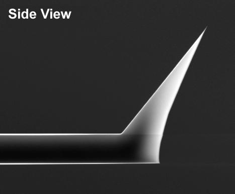
NANOSENSORS AdvancedTEC AFM Probe SEM image Side View
The Platinum Iridium and the gold coated AdvancedTEC™ AFM probes will be available in different force constants and resonant frequencies for contact mode, non-contact/tapping mode and force modulation mode measurements.
These new variations extend the range of applications for the AdvancedTEC to Electrostatic Force Mode (EFM), Scanning ElectroChemical Microscopy (SECM), Scanning Capacitance Mode (SCM), Scanning Kelvin Probe Microscopy (SKPM) as well as to usage in combined imaging techniques such as: Atomic Force Microscopy (AFM) – Scanning Electron Microscopy (SEM) imaging, Infra Red – Scanning Nearfield Optical Microscopy (IR-SNOM) or Electrical Micro-Nanprober systems.
The gold coated AdvancedTEC™ is especially interesting for applications in the fields of Biology and Life Sciences like Force Spectroscopy, Binding Force Spectroscopy (Pull-off measurements) and chemical spectroscopy.
The general advantage of the AdvancedTEC is that this highly doped monolithic silicon probe is designed for precise positioning and high resolution imaging. It features a rectangular cantilever with a triangular free end and a tetrahedral tip that protrudes from the very end of the cantilever. This unique feature allows precise positioning and makes the AdvancedTEC™ the only scanning probe in the world that offers real tip visibility through the optical system of the Atomic Force Microscope – even when the probe is slightly tilted due to its mounting. This makes it the premium choice for all applications where the tip has to be visible (e.g. nanomanipulation). The AdvancedTEC™ Tip is defined by real crystal planes which results in highly reproducible geometries and extremely smooth surfaces. Due to its very small half cone angles this new tip also shows great performance on samples that have a small pattern size combined with steep side walls.
The AdvancedTEC™ is especially interesting for all applications where a direct optical access from top or from the side is necessary in order to be able to illuminate the AFM probe, the AFM tip or the sample simultaneously with the measurement with a laser, electron beam etc.
NANOSENSORS
Rue Jaquet-Droz 1
C.P. 216
2002 Neuchatel
Switzerland
Presscontact: Michaela Roessger Head of Marketing
Email: roessger@nanosensors.com
Phone: +41-(0)32-720-5085
About NANOSENSORS™:
Since more than 15 years researchers world-wide rely on the guaranteed high quality of NANOSENSORS™ probes for Atomic Force Microscopy and Scanning Probe Microscopy.
NANOSENSORS™ AFM tips are mainly used in university research and commercial R&D labs where high resolution, consistent quality and reproducibility of results are essential.
NANOSENSORS™ products are especially designed for the needs of scientists in the fields of nanotechnology, microtechnology, materials research, semiconductors, biology, biotechnology, chemistry and medicine.
NANOSENSORS™ is a trademark of NanoWorld AG.
This release was published on openPR.
Permanent link to this press release:
Copy
Please set a link in the press area of your homepage to this press release on openPR. openPR disclaims liability for any content contained in this release.
You can edit or delete your press release NANOSENSORS™ introduces AdvancedTEC AFM Probes with Gold and Platinum Coating here
News-ID: 44798 • Views: …
More Releases from NANOSENSORS

Global Nanosensors Market Expected To Reach At A CAGR Of 92.81% Between The Peri …
Researchmoz added Most up-to-date research on "Global Nanosensors Market Expected To Reach At A CAGR Of 92.81% Between The Period 2017 - 2021" to its huge collection of research reports.
Nanosensors are any organic, synthetic, or surgical tactile focus or sensory points used to transfer data about nanoparticles to the naturally visible world. Their utilization primarily incorporates different therapeutic purposes, and they serve as gateways to building a variety of nanoproducts.…
Nanosensors Global Market Analysis, Size, Share, Growth, Trends and Forecast Rep …
Researchmoz added Most up-to-date research on "Nanosensors Market by Product Type (Optical, Electrochemical, Electromagnetic), by Application (Automotive & Aerospace, Homeland Defense & Military, Biomedical & Healthcare) - Global Industry Analysis, Size, Share, Growth, Trends and Forecast 2015 - 2021" to its huge collection of research reports.
Nanosensors are defined as any surgical, biological or chemical points that are used to convey information about nanoparticles to macroscopic world. These are mainly…
NANOSENSORS introduces self-sensing self-actuating Akiyama-Probe
Neuchâtel, November 10, 2008 - The Akiyama-probe has been developed in cooperation with the Institute of Microtechnology (IMT) at the University of Neuchâtel for the NANOSENSORS™ brand that is specialized on cutting edge scanning probes for Atomic Force Microscopy (AFM) applications. The product is called the Akiyama-probe or A-probe to honour its inventor Dr. Terunobu Akiyama. It is a novel self-sensing and – actuating probe based on a quartz tuning…
