


Press release
Why is a CVD coating focus ring for etching critical for high-precision semiconductor etching?
. From Plasma Etching to Focused Ring Engineering
Plasma etching is one of the most critical patterning technologies in modern semiconductor manufacturing, enabling the creation of the nanoscale features required for advanced logic and memory devices. As technology nodes continue to shrink below 10 nanometers and device architectures evolve toward FinFET and Gate-All-Around (GAA) structures, the tolerance for process variations has narrowed dramatically. Today, parameters such as etch uniformity, critical dimension (CD) control, and defect density must be controlled with near-atomic precision.
While process optimization typically focuses on plasma chemistry, radio frequency (RF) power, and chamber design, an equally important-yet often less prominent-factor lies in the control of boundary conditions at the wafer edges. This is precisely where the focus ring plays a critical role. Located around the wafer on the electrostatic chuck (ESC), the focus ring acts as a boundary modifier, reshaping the local electric field, stabilizing the plasma sheath, and ensuring uniform ion distribution across the entire wafer surface.
In advanced etching environments, focus rings coated with chemical vapor deposition (CVD) have become the industry standard due to their superior material properties. These components are not merely consumables; they are precision-engineered surfaces that directly influence plasma behavior, process stability, and ultimately determine device yield.
. Why Focus Rings Are Critical in High-Precision Etching
In plasma etching systems, the wafer edges exhibit discontinuities in both geometry and electrical boundary conditions. Without proper compensation measures, this discontinuity leads to significant distortions in the electric field and plasma sheath, triggering the so-called "edge effect." This effect manifests as non-uniform ion incidence angles and fluctuations in ion flux density, resulting in deviations in etch rates and etch profiles near the wafer edge.
Experimental and theoretical studies indicate that, in the absence of edge compensation structures, the region extending several millimeters inward from the wafer edge becomes an unusable edge zone. For advanced technology nodes, where chip sizes are large and process margins are extremely tight, such area loss is economically unacceptable.
The introduction of a focusing ring effectively extends the plasma boundary outward beyond the physical edge of the wafer, thereby creating a more uniform sheath structure. By providing a controlled electrical and physical environment, the focusing ring ensures that the trajectories of ions remain highly consistent across the entire wafer surface. This is critical for achieving the uniformity levels required by modern mass production; in such manufacturing environments, the target for in-wafer etch uniformity is typically set within a range of plus-minus 2%.
Furthermore, by stabilizing the boundary conditions of the chamber across different wafers, the focusing ring helps improve process repeatability. In high-throughput manufacturing environments, even minor fluctuations in edge conditions can lead to cumulative process drift; therefore, the stability of focus ring performance is particularly indispensable.
. The Core Value of CVD Coatings
As plasma etching processes become increasingly demanding-particularly with the widespread adoption of fluorine- and chlorine-based chemical processes-the material requirements for focus rings have also become more stringent. Traditional materials such as quartz or bulk ceramics often suffer from high etch rates, a tendency to generate particles, and poor stability under long-term plasma exposure. CVD coatings-particularly CVD SiC (silicon carbide) and CVD carbon coatings-effectively overcome these limitations thanks to their unique microstructure and chemical properties.
A key characteristic of CVD coatings is their extremely high density, which is close to the theoretical density, and their extremely low porosity, which greatly enhances their resistance to plasma-induced etching. Studies have shown that in a fluorine-based plasma environment, the etch rate of CVD SiC is only a fraction of that of quartz, making it an ideal material for long-duration, high-power etching processes. This increased durability directly translates to longer component lifespans and reduced maintenance frequency.
Equally important is the issue of contamination control. Particles generated by chamber components remain one of the primary causes of yield loss in advanced semiconductor manufacturing processes. According to SEMI standards and relevant contamination control studies, even sub-micron particles can cause critical defects, particularly in advanced process nodes below 10 nanometers. CVD coatings, with their dense and stable surface properties, significantly reduce the risk of surface micro-spalling and impurity release, thereby helping to create a cleaner process environment and improve yield.
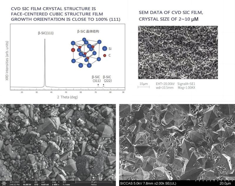
Image: https://www.vet-china.com/uploads/CVD-SiC-Film-Crystal-and-Micro-Structure.jpg [https://www.vet-china.com/cvd-coating/]
CVD SiC Film Crystal and Micro Structure
Another critical aspect is the control of secondary electron emission (SEE). The interaction between the plasma and the chamber surface is strongly influenced by SEE characteristics, which in turn affect plasma density and stability. Compared to traditional materials, CVD-coated surfaces exhibit more consistent and predictable SEE characteristics, enabling more precise control of plasma conditions and improving process repeatability.
Thermal stability is another key advantage of CVD coatings. High-density plasma processes often generate significant thermal loads, particularly in the wafer edge regions. Materials such as CVD SiC possess excellent thermal conductivity and controllable thermal expansion properties, effectively reducing the risk of cracking, warping, or delamination under cyclic thermal stress. This structural integrity is critical for ensuring consistent performance throughout extended process cycles.
. Impact on Key Etching Performance Metrics
Integrated CVD Coating Focus Ring
This focus ring will have a direct and quantifiable impact on multiple key performance metrics in semiconductor etching processes. One of the most critical metrics is etch uniformity. By stabilizing the plasma sheath and ensuring uniform ion flux distribution, CVD-coated focusing rings enable strict control over wafer-wide uniformity, often achieving the plus-minus 2% precision required for advanced device manufacturing. This level of control is particularly critical for high aspect ratio etching processes, where even minor deviations can lead to severe etch profile distortion.
Critical Dimension (CD) Control
Fluctuations in ion incidence angles at the wafer edges can cause CD deviations, and this issue becomes increasingly challenging as feature sizes continue to shrink. By maintaining consistent electric field conditions, the focusing ring helps ensure uniformity in ion trajectories, thereby reducing CD fluctuations across the entire wafer. This is critical for maintaining device performance and meeting design specifications at advanced process nodes.
Enhancing Process Repeatability and Stability
CVD coatings provide a stable and durable surface whose properties remain consistent over time, thereby reducing plasma condition drift and enabling more consistent performance across wafers. In high-volume manufacturing environments, this is critical for implementing Statistical Process Control (SPC).
Enhanced Particle Control Performance
Reduced wear and improved surface integrity minimize particle generation, which directly impacts yield and device reliability. In advanced semiconductor manufacturing, where defect density control targets are extremely stringent, this advantage alone is sufficient to justify the adoption of CVD-coated components.
As the semiconductor industry's demands for process control precision and material performance continue to rise, the development and supply of CVD-coated focus rings are increasingly concentrated among a select few specialized, technology-driven manufacturers. Companies such as Hexcarbon [https://www.hexcarbon.cn/], Vetek Semiconductor [https://www.veteksemicon.com/], and Semicera [https://www.semi-cera.com/] have established a solid market position in this field through their advanced CVD coating technologies, high-purity material processing capabilities, and deep integration with semiconductor equipment requirements. Specifically, companies like Vetek and Semicera focus on providing customized engineering solutions, tailoring focus ring designs to specific etch chemistry formulations and equipment platforms; while Hexcarbon has built a strong market reputation based on its expertise in high-purity graphite and coated components for semiconductor applications. This combination of materials science expertise and process technology know-how enables these companies to meet the increasingly stringent demands of next-generation semiconductor manufacturing.
References:
Principles of Plasma Discharges and Materials Processing
Journal of Vacuum Science & Technology A
Media Contact
Company Name: Ningbo VET Energy Technology Co., Ltd
Email:Send Email [https://www.abnewswire.com/email_contact_us.php?pr=why-is-a-cvd-coating-focus-ring-for-etching-critical-for-highprecision-semiconductor-etching]
Country: China
Website: https://www.vet-china.com/
Legal Disclaimer: Information contained on this page is provided by an independent third-party content provider. ABNewswire makes no warranties or responsibility or liability for the accuracy, content, images, videos, licenses, completeness, legality, or reliability of the information contained in this article. If you are affiliated with this article or have any complaints or copyright issues related to this article and would like it to be removed, please contact retract@swscontact.com
This release was published on openPR.
Permanent link to this press release:
Copy
Please set a link in the press area of your homepage to this press release on openPR. openPR disclaims liability for any content contained in this release.
You can edit or delete your press release Why is a CVD coating focus ring for etching critical for high-precision semiconductor etching? here
News-ID: 4443905 • Views: …
More Releases from ABNewswire

Unique As You Captures Nationwide Attention with Bold Statement Tees and a Heart …
Unique As You has experienced rapid growth in the statement apparel space, drawing customers who want their clothing to reflect personality and conviction. The company has also committed to supporting Ronald McDonald House Charities, inspired by a deeply personal family experience.
Buffalo, New York, USA - September 25, 2026 - Unique As You, a rising apparel brand specializing in bold statement tees for men and women, today announced a milestone period…

CPG Brands Overlook R&D Tax Credits in Product Development, K-38 Consulting Expl …
K-38 Consulting explains how CPG brands can qualify for R&D tax credits through product development, formulation, packaging, testing, and process improvements. The firm highlights common eligibility misconceptions and recommends reviewing documentation, development expenses, and prior tax years to identify potential savings.
RALEIGH, N.C. - September 25, 2026 - Consumer product companies spend heavily on developing new formulations, testing packaging, and improving shelf life - activities that frequently qualify for the federal…

Curate Launches Integrated Text Messaging for Catering and Event Teams
New two-way SMS capability keeps client conversations connected to the contact records and operational workflows teams already manage in Curate
ST. LOUIS, September 25, 2026 - Curate, an event operations platform for caterers and other special-event businesses, today announced the launch of Curate Texting, a two-way SMS capability that allows teams to send and receive client text messages directly from a Contact profile in Curate.
Curate Texting gives event professionals a shared,…

Best EHR for Solo Therapists With One-Time Payment launched by Easy Mind Care LL …
It is a new HIPAA-compliant management software built exclusively for small mental health practices. It eliminates monthly software fees entirely, and also includes unlimited clients and 100 GB of secure storage, so solo therapists can visit EasyMindCare.com to learn more.
Gastonia, North Carolina - September 25, 2026 - Easy Mind Care LLC today launched its electronic health record (EHR) platform for solo mental health therapists, introducing a one-time $149 "Founder's Club"…
More Releases for CVD
Microwave Generator for CVD Diamonds Market
Microwave Generator for CVD Diamonds Market Overview
The microwave generator has a significant impact on the growth rate, quality, and production efficiency of CVD diamonds by controlling plasma generation, temperature, uniformity, and stability.Therefore, when selecting and designing a microwave generator, multiple factors need to be considered to ensure that it can meet the needs of diamond growth.
This report provides a deep insight into the global Microwave Generator for CVD Diamonds market…
Graphene CVD Equipment Market Size, Potential Scope 2031 By Key Players- Quantum …
𝐔𝐒𝐀, 𝐍𝐞𝐰 𝐉𝐞𝐫𝐬𝐞𝐲: According to Verified Market Reports analysis, the global Graphene CVD Equipment Market size was valued at USD 115.77 Million in 2023 and is projected to reach USD 281.41 Million by 2031, growing at a CAGR of 13.5% from 2024 to 2031.
What is the current market outlook for the Graphene CVD Equipment Market?
The Graphene Chemical Vapor Deposition (CVD) Equipment Market is expected to experience significant growth, driven by increasing demand…
CVD Diamond Coating Service Market Size, Share and Forecast By Key Players-SP3 D …
𝐔𝐒𝐀, 𝐍𝐞𝐰 𝐉𝐞𝐫𝐬𝐞𝐲- According to the MRI Team's Market Research Intellect, the global CVD Diamond Coating Service market is anticipated to grow at a compound annual growth rate (CAGR) of 7.97% between 2024 and 2031. The market is expected to grow to USD 8.1 Billion by 2024. The valuation is expected to reach USD 13.84 Billion by 2031.
The market for CVD (Chemical Vapor Deposition) diamond coating services is expanding significantly because to the growing…
Semiconductor Chemical Vapor Deposition (CVD) Equipment Market 2020 Precise Outl …
The Semiconductor Chemical Vapor Deposition (CVD) Equipment Market report is a valuable source of insightful data for business strategists. It provides the industry overview with growth analysis and historical & futuristic cost, revenue, demand, and supply data. The research analysts provide an elaborate description of the value chain and its distributor analysis. This Market study provides comprehensive data that enhances the understanding, scope, and application of this report.
Semiconductor Chemical Vapor…
CVD Diamond Sales Market: The global CVD diamond sales will grow at a CAGR of 7. …
The Global CVD Diamond Sales Market 2020 Report offers entire data on the CVD Diamond Sales market. The report covers the major components such as main players, analysis, size, the situation of the business, SWOT analysis, best techniques of production, management, and marketing. Also, the report sports data in the form of tables, numbers, and charts which offer a clear view of the CVD Diamond Sales market. The latest data…
Global CVD SiC Market Outlook (2014-2025)
The global CVD SiC market is valued at 130 million US$ in 2018 is expected to reach 240 million US$ by the end of 2025, growing at a CAGR of 7.3% during 2019-2025.
This report focuses on CVD SiC volume and value at global level, regional level and company level. From a global perspective, this report represents overall CVD SiC market size by analyzing historical data and future prospect. Regionally, this…

