


Press release
Wafer Level Low-Loss Materials Market Analysis: How Dielectric Innovation Is Minimizing Signal Loss in Next-Generation Semiconductor Devices

Market Growth Trajectory: The Foundation of High-Frequency Semiconductor Performance
The global market for wafer level low-loss materials was valued at US$ 3.23 billion in 2024 and is projected to reach a readjusted size of US$ 5.17 billion by 2031, reflecting a robust compound annual growth rate (CAGR) of 7.0% during the forecast period from 2025 to 2031. This accelerated growth trajectory is driven by the semiconductor industry's relentless pursuit of higher-frequency performance for 5G communications, millimeter-wave (mmWave) applications, advanced RF devices, and next-generation integrated circuits-applications where signal integrity and minimal propagation loss are paramount to device functionality.
Wafer-level low-loss materials are essential in the fabrication of semiconductor devices, especially in applications that require high-frequency performance, such as 5G communications, RF (radio frequency) devices, and advanced integrated circuits. These materials are characterized by their ability to minimize signal loss-a critical requirement as operating frequencies extend into the mmWave spectrum (24 GHz and above), where dielectric losses in conventional materials can degrade signal integrity, increase power consumption, and limit device performance. This material property addresses a fundamental industry pain point: the inability of traditional polymer dielectrics and silicon dioxide interlayer dielectrics to maintain acceptable loss tangents at frequencies exceeding 10 GHz, necessitating the adoption of advanced low-loss alternatives.
【Get a free sample PDF of this report (Including Full TOC, List of Tables & Figures, Chart)】
https://www.qyresearch.com/reports/4428695/wafer-level-low-loss-materials
Industry Analysis: The Science Behind Low-Loss Material Performance
The market analysis landscape for wafer level low-loss materials reveals a technology sector that is becoming increasingly critical as semiconductor devices migrate to higher frequencies. At the wafer level-during the fabrication of integrated circuits, RF front-end modules, and advanced packaging-materials are deposited as interlayer dielectrics, passivation layers, and redistribution layers (RDLs). The dielectric properties of these materials, particularly the dissipation factor (Df) and dielectric constant (Dk), directly determine signal propagation characteristics.
Wafer level low-loss materials are engineered to achieve Df values below 0.005 at operating frequencies up to 100 GHz, with Dk tightly controlled to maintain consistent impedance across device structures. Advanced formulations include specialized thermosets, thermoplastics, and ceramic-filled composites that balance low dielectric loss with the mechanical and thermal properties required for semiconductor processing. The integration of these materials into wafer-level processing-including spin coating, lamination, and chemical mechanical planarization (CMP)-requires precise control of material characteristics to maintain compatibility with existing fabrication flows.
Trends Analysis: Key Developments Shaping the Wafer Level Low-Loss Materials Market
Several significant trends analysis indicators are shaping the wafer level low-loss materials landscape. First, the global deployment of 5G infrastructure and the proliferation of 5G-enabled smartphones represent the largest growth catalysts. According to recent industry data, global 5G smartphone shipments exceeded 750 million units in 2024, with penetration exceeding 65% of total smartphone shipments. Each 5G device requires advanced RF front-end modules (FEMs) that incorporate multiple power amplifiers, switches, and filters-all fabricated using wafer level low-loss materials to achieve the linearity, efficiency, and isolation required for complex modulation schemes.
Second, the transition to mmWave 5G (FR2 bands) is intensifying material performance requirements. Unlike sub-6 GHz 5G (FR1), mmWave frequencies impose significantly tighter constraints on dielectric loss, as signal attenuation increases exponentially with frequency. Recent mmWave deployment milestones-including commercial availability of mmWave 5G in over 100 cities globally-have accelerated the adoption of ultra-low-loss material formulations.
Third, the emergence of advanced packaging technologies-including fan-out wafer-level packaging (FOWLP) and 2.5D/3D integration-is creating new demand for wafer level low-loss materials. These packaging approaches require redistribution layers (RDLs) that must maintain signal integrity across multiple layers and interconnects, driving the adoption of low-loss dielectrics with precise thickness uniformity and planarization characteristics.
Segment Analysis: Material Types and Application Dynamics
By Material Type:
Thermoset: Thermoset-based wafer level low-loss materials-including polyimides, benzocyclobutene (BCB), and advanced epoxy formulations-represent the largest market segment. These materials offer excellent thermal stability, chemical resistance, and mechanical properties compatible with semiconductor processing. Thermosets are widely deployed as interlayer dielectrics and passivation layers in RF device fabrication.
Thermoplastics: Thermoplastic wafer level low-loss materials, including liquid crystal polymers (LCP) and fluoropolymer-based formulations, offer ultra-low dielectric loss and moisture absorption characteristics. These materials are increasingly specified for mmWave applications where minimal loss is critical.
Ceramics: Ceramic-based low-loss materials, including alumina, aluminum nitride, and low-temperature co-fired ceramic (LTCC) formulations, provide exceptional thermal conductivity and dimensional stability. These materials are deployed in high-power RF applications and advanced packaging structures.
Glass: Glass-based wafer level low-loss materials are emerging as enabling substrates for advanced packaging, offering ultra-flat surfaces, CTE matching with silicon, and low dielectric loss characteristics. Glass interposers are gaining traction in high-performance computing and RF applications.
By Application:
Infrastructure: The infrastructure segment encompasses 5G base stations, small cells, and backhaul equipment. These applications demand wafer level low-loss materials capable of handling high-power RF transmission while maintaining signal integrity across wide temperature ranges.
Smartphone: The smartphone segment represents the largest volume application for wafer level low-loss materials, driven by the integration of increasingly complex RF front-end modules. Each 5G smartphone incorporates multiple RF components fabricated with low-loss materials, including power amplifiers, switches, filters, and antenna tuning modules.
Customer Premises Equipment (CPE): CPE applications include fixed wireless access (FWA) devices, residential gateways, and enterprise networking equipment. The expansion of 5G FWA as a broadband alternative-with subscriber growth exceeding 30% annually-is driving sustained demand for low-loss material solutions.
Competitive Landscape: Global Industry Leaders
The wafer level low-loss materials market features a concentrated competitive landscape with specialized chemical and advanced materials companies. Key participants include:
DuPont: A global leader in electronic materials with comprehensive portfolios of low-loss dielectrics for wafer-level processing, including advanced polyimides and fluoropolymer formulations.
Toray Industries: A Japanese materials leader with extensive capabilities in low-loss thermosets and specialty polymers for semiconductor applications.
Showa Denko: A Japanese chemical company with advanced low-loss material formulations for RF device fabrication.
Taiyo Ink: A specialist in photosensitive dielectrics and low-loss materials for semiconductor packaging applications.
HD Microsystems: A joint venture between DuPont and Hitachi, specializing in polyimide-based low-loss materials for advanced packaging.
Ajinomoto: A diversified chemical company with significant presence in build-up film materials, including low-loss formulations for advanced packaging.
Sartomer (Arkema): A specialty chemical company with expertise in acrylate and epoxy-based low-loss materials for semiconductor applications.
AGC Chemicals: A fluoropolymer specialist with ultra-low-loss materials for mmWave applications.
Mitsubishi Gas Chemicals: A Japanese chemical manufacturer with low-loss material portfolios for semiconductor processing.
Technical Challenges and Innovation Frontiers
Despite strong market momentum, the wafer level low-loss materials industry faces technical challenges driving innovation. Process integration remains critical, as low-loss materials must be compatible with existing semiconductor fabrication processes-including photolithography, etching, and metal deposition-without compromising yield or reliability. Manufacturers are developing formulations with optimized photosensitivity and planarization characteristics to simplify integration.
Reliability under environmental stress presents another engineering frontier. Wafer level low-loss materials must maintain stable dielectric properties across temperature extremes, humidity exposure, and thermal cycling conditions. Industry leaders are developing advanced material architectures with improved moisture resistance and thermal stability.
Market Outlook and Future Prospects
The industry outlook for wafer level low-loss materials remains exceptionally positive through the 2031 forecast horizon. Several factors support continued market expansion. First, the transition to 6G research and development is establishing performance roadmaps that will require even lower dielectric loss materials. Second, the proliferation of automotive radar, satellite communications, and mmWave sensing applications will expand addressable markets. Third, continued investment in advanced packaging technologies will create sustained demand for low-loss dielectrics.
Conclusion
As the semiconductor industry pushes toward higher frequencies and more demanding RF performance requirements, wafer level low-loss materials stand as essential enabling technologies. With a projected market valuation of US$5.17 billion by 2031 and sustained 7.0% CAGR growth, the wafer level low-loss materials market represents one of the most dynamic and strategically important segments within the semiconductor materials industry.
About Us:
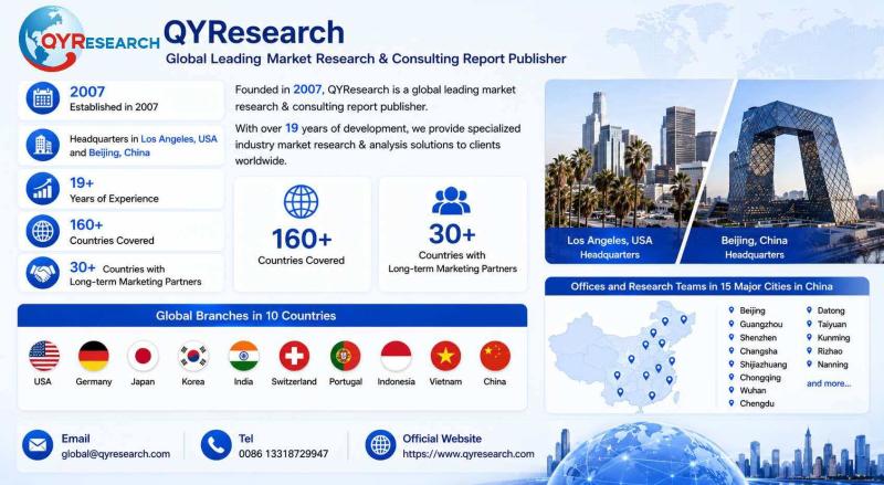
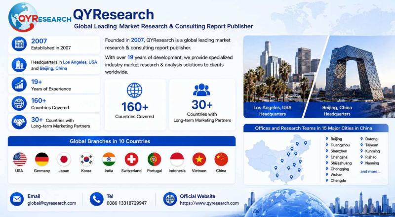
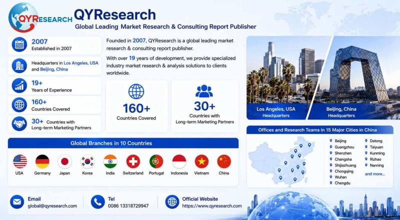
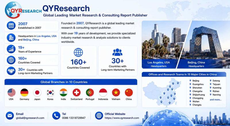
QYResearch founded in California, USA in 2007, which is a leading global market research and consulting company. Our primary business include market research reports, custom reports, commissioned research, IPO consultancy, business plans, etc. With over 19 years of experience and a dedicated research team, we are well placed to provide useful information and data for your business, and we have established offices in 7 countries (include United States, Germany, Switzerland, Japan, Korea, China and India) and business partners in over 30 countries. We have provided industrial information services to more than 60,000 companies in over the world.
Contact Us:
If you have any queries regarding this report or if you would like further information, please contact us:
QY Research Inc.
Add: 17890 Castleton Street Suite 369 City of Industry CA 91748 United States
EN: https://www.qyresearch.com
E-mail: global@qyresearch.com
Tel: 001-626-842-1666(US)
JP: https://www.qyresearch.co.jp
This release was published on openPR.
Permanent link to this press release:
Copy
Please set a link in the press area of your homepage to this press release on openPR. openPR disclaims liability for any content contained in this release.
You can edit or delete your press release Wafer Level Low-Loss Materials Market Analysis: How Dielectric Innovation Is Minimizing Signal Loss in Next-Generation Semiconductor Devices here
News-ID: 4438889 • Views: …
More Releases from QY Research Inc.
Keyless Bluetooth Car Key Research:market size is projected to reach USD 2.48 bi …
The global market for Keyless Bluetooth Car Key was estimated to be worth US$ 867 million in 2025 and is projected to reach US$ 2481 million, growing at a CAGR of 16.1% from 2026 to 2032.
Global Market Research Publisher QYResearch (QY Research) announces the release of its latest report "Keyless Bluetooth Car Key - Global Market Share and Ranking, Overall Sales and Demand Forecast 2026-2032". Based on 2025 market situation…
Industrial Protocol Conversion Gateway Integration Service Research:CAGR of 6.8% …
The global market for Industrial Protocol Conversion Gateway Integration Service was estimated to be worth US$ 2950 million in 2025 and is projected to reach US$ 4676 million, growing at a CAGR of 6.8% from 2026 to 2032.
Global Market Research Publisher QYResearch (QY Research) announces the release of its latest report "Industrial Protocol Conversion Gateway Integration Service - Global Market Share and Ranking, Overall Sales and Demand Forecast 2026-2032". Based…
Industrial Ammonia Catalyst Research:CAGR of 4.0% during 2026-2032
The global market for Industrial Ammonia Catalyst was estimated to be worth US$ 188 million in 2025 and is projected to reach US$ 246 million, growing at a CAGR of 4.0% from 2026 to 2032.
Global Market Research Publisher QYResearch (QY Research) announces the release of its latest report "Industrial Ammonia Catalyst - Global Market Share and Ranking, Overall Sales and Demand Forecast 2026-2032". Based on 2025 market situation and impact…
HPP Juice Research: CAGR of 7.6% during the forecast period
The global market for HPP Juice was estimated to be worth US$ 1639 million in 2025 and is projected to reach US$ 2864 million, growing at a CAGR of 8.6% from 2026 to 2032.
Global Market Research Publisher QYResearch (QY Research) announces the release of its latest report "HPP Juice - Global Market Share and Ranking, Overall Sales and Demand Forecast 2026-2032". Based on 2025 market situation and impact historical analysis…
More Releases for Wafer
Wafer Surface Thinning Machine Market 2026-2032: Fully Automatic Wafer Grinders, …
Global Leading Market Research Publisher QYResearch announces the release of its latest report "Wafer Surface Thinning Machine - Global Market Share and Ranking, Overall Sales and Demand Forecast 2026-2032". For semiconductor fabs, OSATs (outsourced semiconductor assembly and test providers), and institutional investors tracking advanced packaging, the wafer back-grinding process has emerged as a critical bottleneck and differentiator. As 3D stacking, fan-out wafer-level packaging (FOWLP), and power device miniaturization intensify, the…
Semiconductor Silicon Wafer Market Is Going to Boom |• Silicon Wafer • Globa …
Worldwide Market Reports has released a new in-depth research study on the "Semiconductor Silicon Wafer Market," highlighting strong growth potential in the coming years. The report delivers a structured and data-driven analysis of the market landscape, combining robust research methodology, market sizing, validated data modeling, and insights sourced from reliable primary and secondary channels.
The study thoroughly examines key market aspects, including growth drivers, restraints, challenges, emerging opportunities, technological advancements, innovation…
Wafer Hybrid Bonding Equipment Market Share Driven by Wafer-to-Wafer Technology …
Wafer Hybrid Bonding Equipment Market Size
The global market for Wafer Hybrid Bonding Equipment was valued at US$ 164 million in the year 2024 and is projected to reach a revised size of US$ 756 million by 2031, growing at a CAGR of 24.7% during the forecast period.
View sample report
https://reports.valuates.com/request/sample/QYRE-Auto-31W14822/Global_Wafer_Hybrid_Bonding_Equipment_Market_Insights_Forecast_to_2029
The Wafer Hybrid Bonding Equipment market is experiencing accelerated growth, driven by increasing demand for advanced semiconductor packaging technologies that enable higher…
Semiconductor Wafer Electrostatic Chucks for 300mm Wafer Market
Semiconductor Wafer Electrostatic Chucks for 300mm Wafer Market
The global Semiconductor Wafer Electrostatic Chucks for 300mm Wafer market was valued at US$ 1165 million in 2023 and is anticipated to reach US$ 1672.7 million by 2030, witnessing a CAGR of 5.3% during the forecast period 2024-2030.
View Sample Report
https://reports.valuates.com/request/sample/QYRE-Auto-38F13137/Global_Semiconductor_Wafer_Electrostatic_Chucks_for_300mm_Wafer_Market_Research_Report_2023
Report Scope
The Semiconductor Wafer Electrostatic Chucks for 300mm Wafer market size, estimations, and forecasts are provided in terms of output/shipments (Units) and revenue…
Automatic Mounter Wafer Equipment Market Report 2018: Segmentation by Type (100 …
Global Automatic Mounter Wafer Equipment market research report provides company profile for Lintec Corporation, Nitto Denko, Tokyo Electron, Technovision, Takatori, Ultron Systems, DISCO Corp., Syagrus Systems, Advanced Dicing Technologies, Longhill Industries and Others.
This market study includes data about consumer perspective, comprehensive analysis, statistics, market share, company performances (Stocks), historical analysis 2012 to 2017, market forecast 2018 to 2025 in terms of volume, revenue, YOY growth rate, and CAGR for…
EMEA Solar Wafer Cutting Fluid PEG Market For Semiconductor, Solar Wafer, Crysta …
Latest industry research report on: EMEA (Europe, Middle East and Africa) Solar Wafer Cutting Fluid PEG Market : Industry Size, Share, Research, Reviews, Analysis, Strategies, Demand, Growth, Segmentation, Parameters, Forecasts
Request For Sample Report @ https://www.marketresearchreports.biz/sample/sample/1194694
Geographically, this report split EMEA into Europe, the Middle East and Africa, With sales (K MT), revenue (Million USD), market share and growth rate of Solar Wafer Cutting Fluid PEG for these regions, from 2012 to…

