Press release
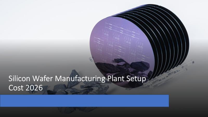
Cost of Setting Up a Silicon Wafer Manufacturing Plant & DPR 2026
Market Overview and Growth Potential
The global silicon wafer market demonstrates a robust and sustained growth trajectory, valued at USD 27.80 Billion in 2025. According to IMARC Group estimates, the market is expected to reach USD 46.71 Billion by 2034, exhibiting a CAGR of 5.64% from 2026 to 2034. This expansion is primarily driven by the expanding demand for semiconductors across electronics, automotive, renewable energy, and data infrastructure sectors. The rapid proliferation of electric vehicles is a key demand driver, with annual global EV sales projected to exceed 20 million units in 2025 alone according to the International Energy Agency (IEA). Renewable energy systems, data centers, artificial intelligence workloads, and automation-intensive manufacturing are further boosting demand for semiconductors delivering high efficiency, thermal stability, and precision.
Request for Sample Report: https://www.imarcgroup.com/silicon-wafer-manufacturing-plant-project-report/requestsample
A silicon wafer refers to a thin, highly pure, and circular slice of single-crystal silicon that constitutes the basic substrate material from which integrated circuits, microprocessors, and solar cells are made. Silicon is a critical semiconductor material whose conductivity can be intentionally enhanced by introducing impurities through a process known as doping. This enables etching of billions of microscopic transistors on the wafer surface through photolithography, etching, and deposition processes. Silicon wafers serve as the universal substrate for integrated circuit fabrication, MEMS devices, power semiconductors, RF components, and photovoltaic cells across the entire global electronics and energy industries.
The Asia-Pacific region, led by China, Taiwan, South Korea, and India, is expected to remain the fastest-growing market due to expanding semiconductor fabrication capacity and strong government support. North America and Europe continue to benefit from investments in domestic chip manufacturing, technology upgrades, and stringent quality standards, with semiconductor incentive programs including the US CHIPS Act and European Chips Act driving new wafer manufacturing capacity investment in regions previously dependent on Asian supply chains for this strategically critical material.
Plant Capacity and Production Scale
The proposed silicon wafer manufacturing facility is designed with an annual production capacity ranging between 3-5 million wafers, enabling economies of scale while maintaining operational flexibility across wafer diameter specifications from 150mm through 300mm and product grades from standard polished wafers to epitaxial, SOI, and specialty substrate products. This capacity range allows manufacturers to serve diverse market segments including semiconductor manufacturing, electronics, photovoltaics, MEMS, and telecommunications - ensuring steady demand and consistent revenue streams driven by expanding logic and memory chip fabrication capacity, growing power semiconductor demand for EV and renewable energy applications, accelerating MEMS sensor adoption, and increasing RF semiconductor requirements for 5G infrastructure deployment worldwide.
Speak to an Analyst for Customized Report: https://www.imarcgroup.com/request?type=report&id=15099&flag=C
Financial Viability and Profitability Analysis
The silicon wafer manufacturing business demonstrates strong profitability potential under normal operating conditions. The financial projections reveal:
• Gross Profit: 45-55%
• Net Profit: 20-25%
These margins reflect the high technological sophistication and precision manufacturing requirements of silicon wafer production, where high-purity polysilicon feedstock is transformed through crystal growth, slicing, polishing, and cleaning into specification-grade wafer substrates commanding significant price premiums in semiconductor fabrication markets. Margins are supported by stable and growing demand across all major semiconductor end-use markets; high barriers to entry from cleanroom infrastructure requirements, crystal growth expertise, and customer qualification cycles that protect established producers from competition; long-term supply agreements with semiconductor fabricators providing revenue visibility; and the strategic supply chain localization investment cycles driven by government semiconductor incentive programs creating new demand opportunities for regional wafer producers. The project demonstrates solid return on investment (ROI) potential with comprehensive financial analysis covering income projections, expenditure projections, break-even points, net present value (NPV), internal rate of return, and detailed profitability and sensitivity analysis. Polysilicon cost management and utility cost optimization - particularly ultra-pure water and electricity for crystal growth furnaces - are the most critical operational success factors for maintaining target margin performance.
Cost of Setting Up a Silicon Wafer Manufacturing Plant:
Understanding the operating expenditure (OpEx) is crucial for effective financial planning and cost management.
Operating Cost Structure
The cost structure for a silicon wafer manufacturing plant is primarily driven by:
• Raw Materials: 40-50% of total OpEx
• Utilities: 30-35% of OpEx
• Other Expenses: Including transportation, packaging, salaries and wages, depreciation, taxes, and other expenses
Raw materials - particularly high-purity polysilicon feedstock - account for approximately 40-50% of total operating expenses, making polysilicon procurement strategy, supplier qualification, and long-term supply contract management the primary raw material cost determinant. Electronic-grade polysilicon with purity levels exceeding 9N (99.9999999%) is the critical feedstock for Czochralski crystal growth, with polysilicon price volatility driven by global supply-demand dynamics directly impacting wafer manufacturing cost competitiveness. Utilities represent an exceptionally high 30-35% of OpEx - substantially above most manufacturing industries - driven by enormous electricity consumption for crystal growth furnaces operating at temperatures exceeding 1,400°C, ultra-pure water (UPW) systems for wafer cleaning operations, and HVAC systems maintaining cleanroom environments at ISO Class 1-5 levels. This elevated utility cost profile reflects the energy-intensive nature of silicon crystal growth and the stringent cleanliness requirements of semiconductor substrate manufacturing. In the first year of operations, costs cover raw materials, utilities, depreciation, taxes, packing, transportation, and repairs and maintenance. Securing stable long-term electricity supply agreements at competitive industrial tariffs and ultra-pure water generation infrastructure are therefore critical capital and operational planning priorities.
Capital Investment Requirements
Setting up a silicon wafer manufacturing plant requires very substantial capital investment - among the highest of any manufacturing sector - across cleanroom infrastructure, crystal growth systems, and precision processing equipment categories. The total capital investment depends on plant capacity, wafer diameter specification, technology level, and location, covering land acquisition, site preparation, and semiconductor-grade cleanroom manufacturing infrastructure.
Land and Site Development: The location must offer easy access to high-purity polysilicon from certified semiconductor-grade suppliers, along with proximity to target markets including semiconductor foundries, integrated device manufacturers (IDMs), and solar cell manufacturers to minimize logistics costs and transit contamination risk for finished wafers shipped in vacuum-sealed FOUP containers. The site must have robust infrastructure including access to ultra-reliable electrical power supply with grid redundancy for uninterruptible crystal growth furnace operation, high-capacity ultra-pure water generation and distribution systems, high-flow industrial gas supply (nitrogen, argon, hydrogen) for inert atmosphere processing, and chemical waste treatment for semiconductor process chemicals. Compliance with semiconductor manufacturing environmental regulations, ultra-pure water discharge standards, chemical waste disposal requirements, and local zoning laws must be ensured.
Machinery and Equipment: Equipment costs for crystal growth furnaces (Czochralski or float zone), wafer saws, edge grinders, lapping and polishing machines, chemical etching baths, cleaning stations, inspection systems, and packaging automation represent the dominant capital expenditure category in silicon wafer plant investment. Highly specialized, precision semiconductor manufacturing equipment must be selected. Essential equipment includes:
• Czochralski crystal growth furnaces for pulling large-diameter single-crystal silicon ingots from polysilicon melt under precisely controlled temperature and rotation profiles
• Multi-wire diamond saws for slicing silicon ingots into thin wafer discs with controlled thickness uniformity and minimum kerf loss
• Edge grinding and edge profiling machines for wafer edge rounding and notch/flat formation to prevent edge chipping and wafer handling breakage
• Lapping and double-side grinding machines for achieving target wafer thickness, flatness, and total thickness variation (TTV) specifications
• Chemical mechanical polishing (CMP) systems for achieving sub-nanometer surface roughness and mirror-finish surface quality required for semiconductor lithography
• Megasonic and RCA wet cleaning stations, chemical etching baths, and spin-rinse-dry systems for particle, metallic contamination, and native oxide removal, plus automated optical inspection (AOI), laser scanning systems, and surface particle counters for 100% wafer defect and contamination inspection
All machinery must comply with SEMI standards for semiconductor equipment safety, wafer handling, and cleanroom compatibility. ISO Class 1-5 cleanroom environments with laminar airflow, positive pressure, and continuous particle monitoring are mandatory for wafer processing and inspection operations. Automated wafer handling using FOUP cassettes and robotic transfer systems are required to prevent human-originated contamination. The wafer diameter specification and production volume will determine the total capital equipment investment, with 300mm wafer production requiring substantially higher capital investment than 150mm or 200mm wafer lines.
Civil Works: Building construction and plant layout meeting semiconductor cleanroom engineering requirements, with ISO-classified cleanroom bays for crystal growth, slicing, grinding, polishing, cleaning, and inspection operations segregated by cleanliness level. Sub-fab infrastructure for chemical distribution, ultra-pure water distribution, process gas supply, waste chemical neutralization, and vacuum systems must be integrated into the facility design. Vibration-isolated foundations for precision polishing and inspection equipment, seismic isolation for cleanroom structures in earthquake-prone regions, and raised-floor cleanroom layouts for under-floor utility distribution are mandatory semiconductor fab civil infrastructure requirements that significantly increase construction costs above standard industrial facilities.
Other Capital Costs: Costs associated with land acquisition, construction, and utilities including ultra-pure water generation systems, industrial gas supply infrastructure, electrical substation and power conditioning for furnace loads, cleanroom HVAC and filtration systems, and chemical waste treatment plants must be considered in the financial plan. Pre-operative expenses including SEMI certification, customer qualification audits, yield ramp-up program costs, initial working capital for polysilicon procurement and production inventory build, and contingency provisions for crystal growth process development and wafer specification qualification timelines of 12-24 months from facility commissioning to first customer qualification.
Buy Now: https://www.imarcgroup.com/checkout?id=15099&method=2175
Major Applications and Market Segments
Silicon wafer manufacturing outputs serve as the foundational substrate for critical applications across the entire semiconductor and electronics industry:
Semiconductor Fabrication: Wafer handling, cleaning, and polishing systems support the use of silicon wafers as the universal substrate for logic, memory, and analog integrated circuit manufacturing, with the exponentially growing global demand for computing power driven by AI, cloud infrastructure, mobile devices, and the Internet of Things creating sustained and accelerating demand for leading-edge and mature-node silicon wafer supply at all diameter specifications.
Photolithography: Mask aligners, resist coating, and exposure equipment enable the patterning of billions of transistors on silicon wafer surfaces, with semiconductor node advancement from 28nm to 5nm, 3nm, and beyond driving demand for progressively larger diameter wafers (300mm) with tighter flatness, surface quality, and defect density specifications that command premium pricing over legacy diameter wafers.
Etching and Deposition: Chemical vapor deposition (CVD), plasma etching, and thin-film coating processes applied to silicon wafer surfaces create the multilayer device structures that define transistor performance, with power semiconductor applications for EV inverters, renewable energy converters, and industrial motor drives driving strong demand for large-diameter silicon wafers optimized for epitaxial layer deposition and high-voltage power device fabrication.
Testing and Packaging: Inspection tools, probe stations, and die packaging equipment process finished silicon wafers into individual semiconductor dice and packaged integrated circuits, with wafer-level packaging (WLP) and advanced packaging technologies including chiplets and 3D integration driving demand for specialty silicon wafers optimized for advanced packaging process compatibility and interposer applications.
Photovoltaics: Silicon wafers serve as the primary substrate for crystalline silicon solar cells, with the global renewable energy transition driving rapidly expanding demand for both monocrystalline and multicrystalline silicon wafers in solar cell manufacturing, particularly for high-efficiency PERC, TOPCon, and HJT solar cell technologies requiring high-quality Czochralski-grown silicon wafer substrates with controlled resistivity and lifetime specifications.
Why Invest in Silicon Wafer Manufacturing?
Several compelling factors make silicon wafer manufacturing an attractive - though capital-intensive - investment opportunity:
Core Enabler of the Semiconductor Ecosystem: Silicon wafers are the key building block in the production of integrated circuits, power devices, sensors, and memory - essential in consumer electronics, automotive semiconductors, renewable energy applications, data centers, and industrial automation - making silicon wafer manufacturing a strategically indispensable industry with non-cyclical structural demand growth driven by the accelerating digitalization of the global economy.
High but Defensible Entry Barriers: Manufacturing silicon wafers requires enormous capital investment, cleanroom environments, precision crystal growth expertise, state-of-the-art slicing, polishing, and inspection capabilities, and lengthy customer qualification cycles - creating high barriers that protect established manufacturers from less capable competitors and enable sustained premium pricing for qualified, specification-compliant wafer producers.
Strong Alignment with Global Megatrends: The rapid growth of electric vehicles, renewable energy, 5G and AI infrastructure, industrial automation, and IoT is driving steady and accelerating demand for semiconductors and thereby creating prolonged and expanding demand for high-quality silicon wafers, with power electronics and advanced node devices registering particularly strong double-digit demand growth rates that outpace the overall semiconductor market average.
Policy and Strategic Manufacturing Support: Government semiconductor incentive programs including the US CHIPS Act, European Chips Act, Japan semiconductor support programs, and India semiconductor mission are enhancing downstream wafer demand while simultaneously creating investment incentives for new wafer manufacturing capacity through capital subsidies, tax incentives, and preferential utility rate structures that improve investment returns for greenfield and brownfield wafer plant projects.
Supply Chain Localization and Strategic Security: Semiconductor companies require a resilient and geographically diversified wafer supply chain to mitigate geopolitical risks, shorten lead times, and ensure continuity of supplies, creating opportunity for regional wafer producers with strong process control and scalable operations to capture long-term supply agreements from semiconductor manufacturers actively seeking to diversify away from geographically concentrated wafer supply chains.
Manufacturing Process Excellence
The silicon wafer manufacturing process is a highly controlled multi-step operation involving several precision unit operations, ultra-clean material handling stages, and rigorous quality checks at every production stage. The process involves crystal growth, slicing, polishing, and cleaning. The main production steps include:
• Polysilicon feedstock receiving, purity certification verification, and controlled storage under nitrogen atmosphere to prevent oxidation
• Czochralski crystal growth - polysilicon melting in quartz crucible at 1,414°C and controlled seed crystal pulling to grow large-diameter single-crystal silicon ingots with target resistivity and crystal orientation
• Ingot characterization including diameter measurement, resistivity mapping, crystal orientation verification (X-ray diffraction), and oxygen/carbon content analysis
• Multi-wire diamond saw slicing of silicon ingots into thin wafer discs with controlled thickness, bow, and warp within tight specification limits
• Edge grinding and beveling for wafer edge rounding and notch or flat formation to semiconductor industry SEMI M1 standard specifications
• Lapping and double-side grinding for thickness uniformity and flatness improvement, followed by chemical etching for damage layer removal
• Chemical mechanical polishing (CMP) for achieving mirror-finish surface roughness below 0.1nm Ra required for semiconductor device fabrication lithography processes
• Megasonic and multi-step wet chemical cleaning (RCA clean) for particles, metallic ions, and organic contamination removal to semiconductor-grade cleanliness levels
• Automated optical and laser scanning inspection for surface particles, micro-scratches, crystal defects, and dimensional compliance verification, followed by FOUP packaging under nitrogen atmosphere and shipment to semiconductor fabrication customers
The complete process flow encompasses unit operations involved, mass balance and raw material requirements, rigorous quality assurance criteria, and technical tests throughout production. ISO-classified cleanroom protocols, SEMI equipment standards compliance, and comprehensive statistical process control (SPC) for all critical process parameters must be implemented throughout the manufacturing plant. Documentation for crystal growth batch records, wafer traveler traceability, customer specification compliance, and SEMI M-series standard certifications must be maintained throughout all production stages. Customer qualification cycles typically require 12-18 months of data submission and joint testing before a new wafer supplier can be approved as a qualified source for semiconductor fabrication customers.
Industry Leadership
The global silicon wafer industry is highly concentrated among a small number of technically sophisticated manufacturers with decades of crystal growth expertise and deep semiconductor customer relationships. Key industry players include:
• Shin-Etsu Chemical
• SUMCO
• GlobalWafers
• Siltronic
• SK Siltron
These companies serve diverse end-use sectors including semiconductor manufacturing, electronics, photovoltaics, MEMS, and telecommunications, with the top five players collectively accounting for the substantial majority of global silicon wafer supply and maintaining multi-decade customer qualification relationships with leading semiconductor foundries and IDMs that represent the most significant competitive moats in the global semiconductor supply chain.
Recent Industry Developments
May 2025: GlobalWafers launched its USD 3.5 billion silicon wafer manufacturing facility in Sherman, Texas, marking the first fully integrated 12-inch (300mm) wafer production line built in the United States in over two decades. This landmark investment underscores the strategic importance of domestic silicon wafer manufacturing capacity to US semiconductor supply chain security and validates the strong investment thesis for regional wafer production in markets where government semiconductor incentive programs are creating compelling economics for new wafer manufacturing capacity that would not otherwise be justified by purely commercial market returns.
The GlobalWafers Sherman facility represents a defining example of the new era of government-supported semiconductor supply chain localization investments enabled by the US CHIPS and Science Act, with the plant set to produce silicon wafers for customers across the logic, memory, power semiconductor, and specialty device segments of the North American semiconductor ecosystem - demonstrating the strategic and commercial viability of greenfield silicon wafer manufacturing in markets with supportive policy frameworks, reliable utility infrastructure, and access to technically skilled semiconductor manufacturing workforce pools.
Browse Full Report: https://www.imarcgroup.com/silicon-wafer-manufacturing-plant-project-report
About Us:
IMARC Group is a global management consulting firm that helps the world's most ambitious changemakers to create a lasting impact. The company excels in understanding its client's business priorities and delivering tailored solutions that drive meaningful outcomes. We provide a comprehensive suite of market entry and expansion services. Our offerings include thorough market assessment, feasibility studies, company incorporation assistance, factory setup support, regulatory approvals and licensing navigation, branding, marketing and sales strategies, competitive landscape, and benchmarking analyses, pricing and cost research, and procurement research.
Contact Us:
IMARC Group
134 N 4th St. Brooklyn, NY 11249, USA
Email: sales@imarcgroup.com
Tel No: (D) +91 120 433 0800
United States: (+1-201-971-6302)
This release was published on openPR.
Permanent link to this press release:
Copy
Please set a link in the press area of your homepage to this press release on openPR. openPR disclaims liability for any content contained in this release.
You can edit or delete your press release Cost of Setting Up a Silicon Wafer Manufacturing Plant & DPR 2026 here
News-ID: 4410082 • Views: …
More Releases from IMARC Group

IMARC Helium Pricing Report: Northeast Asia Leads at $152.7/MC While Europe Drop …
The global helium market is experiencing sharp fluctuations in March 2026, shifting rapidly from a phase of relative oversupply to renewed tightness. Earlier in the year, increased production from Russia and North America had created a temporary surplus. However, escalating geopolitical tensions in the Middle East have disrupted supply chains, significantly impacting the global helium price outlook.
Constraints in logistics-particularly those affecting exports from Qatar-have triggered notable regional price disparities. While…
Zinc Sulphate Production Plant Setup 2026: Complete DPR with Process Flow, Machi …
Setting up a zinc sulphate manufacturing plant positions investors within one of the most essential and consistently expanding segments of the global inorganic chemicals and agricultural micronutrient industry, supported by increasing demand for zinc-based fertilisers to address widespread soil zinc deficiency, growing adoption of zinc sulphate across water treatment, animal feed supplementation, and pharmaceutical applications, and rising industrial consumption in rayon manufacturing, electroplating, and chemical synthesis operations. Zinc sulphate is…
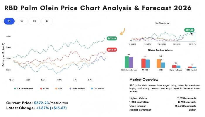
RBD Palm Olein Price Chart 2026 Shows 5% Growth Across Key Global Markets
The RBD Palm Olein price chart in 2026 highlights a dynamic global market influenced by feedstock costs, weather conditions, and export demand from Southeast Asia. Prices have shown moderate volatility due to fluctuating crude palm oil production and shifting global consumption patterns. The RBD Palm Olein market outlook remains cautiously optimistic, supported by strong demand from food processing industries and emerging economies.
Key RBD Palm Olein Price Highlights:
• China: USD 1,020/MT…
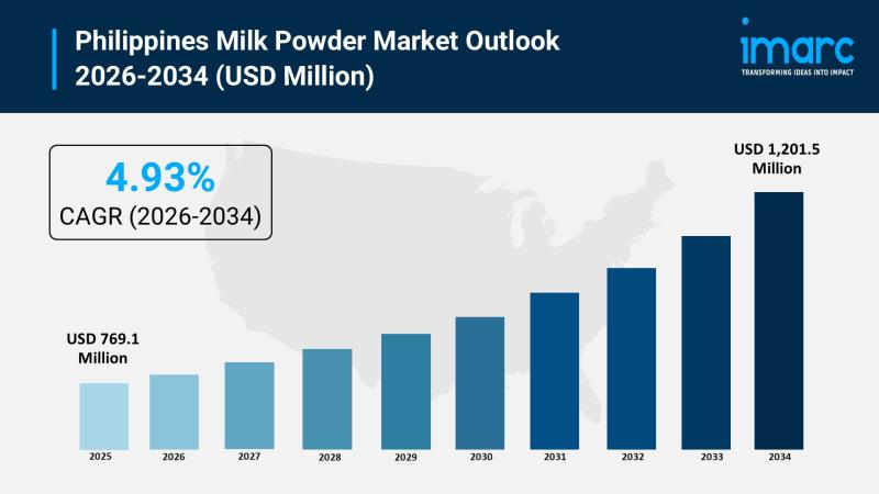
Philippines Milk Powder Market 2026 | Projected to Reach USD 1,201.5 Million by …
Market Overview
The Philippines milk powder market size reached USD 769.1 Million in 2025 and is projected to reach USD 1,201.5 Million by 2034, exhibiting a growth rate (CAGR) of 4.93% during 2026-2034. The market encompasses diverse product types, functions, and applications tailored to the Philippines' evolving dairy and nutrition needs, covering whole milk powder and skimmed milk powder across emulsification, foaming, flavouring, and thickening functions serving infant formula, confectionery, sports…
More Releases for Silicon
Silicon Carbide Ceramics and Silicon Nitride Ceramics
Overview of Silicon Carbide Ceramics [https://www.rbsic-sisic.com/wear-resistant-silicon-carbide-ceramic-tiles-3.html]
Silicon carbide ceramics are a new type of ceramic material made mainly from silicon carbide powder through high-temperature sintering. Silicon carbide ceramics have high hardness, wear resistance, corrosion resistance, and excellent high temperature resistance, with excellent mechanical, thermal, and electrical properties. Silicon carbide ceramics can be divided into compacted sintered silicon carbide ceramics and reaction sintered silicon carbide ceramics due to different firing processes.
Overview of…
High Purity Silicon Metal Market Growth Forecast: Latest Research Unveils Opport …
Global High Purity Silicon Metal Market Overview:
Global High Purity Silicon Metal Market Report 2022 comes with the extensive industry analysis by Introspective Market Research with development components, patterns, flows and sizes. The report also calculates present and past market values to forecast potential market management through the forecast period between 2022-2028.
This research study of High Purity Silicon Metal involved the extensive usage of both primary and secondary data sources. This…
Future Prospects of Silicon Rings and Silicon Electrodes for Etching Market by …
The Silicon Rings and Silicon Electrodes for Etching Market research report provides all the information related to the industry. It gives the outlook of the market by giving authentic data to its client which helps to make essential decisions. It gives an overview of the market which includes its definition, applications and developments and manufacturing technology. This Silicon Rings and Silicon Electrodes for Etching market research report tracks all the…
Silicon Metal Market Global Outlook 2021-2026: Ferroglobe, Mississippi Silicon, …
The Global Silicon Metal Market Research Report 2021-2026 is a valuable source of insightful data for business strategists. It provides the industry overview with growth analysis and historical & futuristic cost, revenue, demand, and supply data (as applicable). The research analysts provide an elaborate description of the value chain and its distributor analysis. This Market study provides comprehensive data which enhances the understanding, scope, and application of this report.
The market…
Global Solar Grade Multi-Crystal Silicon Market Leading Major Players – GCL-Po …
Researchmoz added Most up-to-date research on "Global (United States, European Union and China) Solar Grade Multi-Crystal Silicon Market Research Report 2019-2025" to its huge collection of research reports.
The Solar Grade Multi-Crystal Silicon market report [6 Year Forecast 2019-2025] focuses on Major Leading Industry Players, providing info like company profiles, product type, application and regions, production capacity, ex-factory price, gross margin, revenue, market share and speak to info. Upstream raw materials…
Silicon Metal Market 2018: Top Key Players H.C. Starck, Elkem, Zhejiang Kaihua Y …
Silicon Metal Market Status and Forecast 2025
This Write up presents in detail analysis of Silicon Metal Market especially market drivers, challenges, vital trends, standardization, deployment models, opportunities, future roadmap, manufacturer’s case studies, value chain, organization profiles, Sales Price and Sales Revenue, Sales Market Comparison and strategies.
The Silicon Metal market Report provides a detailed analysis of the Silicon Metal industry. It provides an analysis of the past 5 years and a future forecast till the year…
