Press release
Advanced Packaging Inspection Systems Market Accelerates as Semiconductor Packaging Complexity Drives Demand for Precision Quality Control
Advanced Packaging Inspection Systems Market SizeIn 2024, the global market size of Advanced Packaging Inspection Systems was estimated to be worth US$ 456 million and is forecast to reach approximately US$ 853 million by 2031 with a CAGR of 9.5% during the forecast period 2025-2031.
Get Free Sample: https://reports.valuates.com/request/sample/QYRE-Auto-10W9117/Global_Advanced_Packaging_Inspection_Systems_Market_Outlook_2022
By Application
• IDM
• OSAT
Key Companies
Camtek, Onto Innovation, KLA, Intekplus, Cohu, Semiconductor Technologies & Instruments (STI), Segment by Power, Optical Based Packaging Inspection Systems, Infrared Packaging Inspection Systems
Major Trends
• Rising adoption of optical and infrared inspection technologies
• Increasing demand from advanced semiconductor packaging processes
• Growth of OSAT facilities driving investment in inspection automation
• Higher focus on defect detection for yield optimization
• Expansion of AI-enabled and high-speed inspection platforms
• Strong adoption across Asia-Pacific semiconductor manufacturing hubs
View Full Report: https://reports.valuates.com/market-reports/QYRE-Auto-10W9117/global-advanced-packaging-inspection-systems
Trends Influencing the Growth of the Market
The Advanced Packaging Inspection Systems market is witnessing rapid expansion as semiconductor packaging evolves toward higher complexity, miniaturization, and heterogeneous integration. Modern packaging technologies such as advanced substrate designs, multi-die integration, and high-density interconnects require highly accurate inspection systems to ensure reliability and performance. Inspection solutions play a critical role in identifying defects, improving production yield, and minimizing costly failures in increasingly sophisticated semiconductor manufacturing environments.
From a technology perspective, Optical Based Packaging Inspection Systems remain the dominant segment due to their ability to provide high-speed, non-contact, and highly detailed surface analysis. Optical inspection systems are widely adopted for detecting alignment issues, surface defects, and packaging anomalies in real time, enabling manufacturers to maintain high throughput while ensuring product quality. Infrared Packaging Inspection Systems are gaining momentum as packaging structures become more complex and multi-layered. Infrared inspection enables non-destructive analysis beneath surface layers, allowing manufacturers to detect internal defects such as voids, delamination, and bonding inconsistencies that are difficult to identify using optical methods alone. The combination of optical and infrared technologies is increasingly common as manufacturers pursue comprehensive inspection strategies to address advanced packaging challenges.
From an application perspective, OSAT (Outsourced Semiconductor Assembly and Test) providers represent a significant growth driver due to rising outsourcing of advanced packaging operations by semiconductor companies. OSAT facilities are investing heavily in automated inspection systems to manage high-volume production and maintain competitive yield rates. The IDM (Integrated Device Manufacturer) segment also contributes strongly, as leading semiconductor companies expand in-house packaging capabilities to support differentiated products and advanced performance requirements. As packaging becomes a key differentiator in semiconductor performance, both IDMs and OSATs are prioritizing sophisticated inspection technologies to enhance process control and quality assurance.
Regionally, Asia-Pacific, particularly China, Japan, and South Korea, dominates demand due to its concentration of semiconductor fabrication and packaging facilities. The region's strong electronics manufacturing ecosystem and ongoing investment in advanced packaging technologies drive substantial adoption of inspection systems. North America and Europe remain important markets, supported by research innovation, semiconductor equipment development, and strategic efforts to strengthen domestic semiconductor supply chains. Emerging markets in Southeast Asia and other regions are gradually expanding adoption as semiconductor assembly and packaging operations grow. Insights from leading consulting firms such as McKinsey, Deloitte, KPMG, and PwC indicate that rising demand for advanced computing, artificial intelligence, and high-performance electronics is accelerating investment in advanced packaging technologies, which in turn strengthens the need for high-precision inspection solutions.
Market Share
The Advanced Packaging Inspection Systems market is moderately consolidated, with specialized equipment providers competing through technological innovation, inspection accuracy, and integration capabilities. Key companies including Camtek, Onto Innovation, KLA, Intekplus, Cohu, and Semiconductor Technologies & Instruments (STI) maintain strong market positions by offering advanced optical and infrared inspection platforms tailored to semiconductor packaging requirements. Market share is influenced by system accuracy, throughput, automation capabilities, and compatibility with advanced packaging workflows. Continuous investment in AI-driven defect detection, machine vision technologies, and high-speed data analytics remains central to competitive differentiation as manufacturers seek to improve yield and efficiency in increasingly complex semiconductor production environments.
Purchase Regional Report: https://reports.valuates.com/request/regional/QYRE-Auto-10W9117/Global_Advanced_Packaging_Inspection_Systems_Market_Outlook_2022
Email Id:
Please reach us at sales@valuates.com
Address:
Valuates,
4th Floor,
Balaraj's Arcade,
Whitefield Main road,
Bangalore 560066
Valuates offers an extensive collection of market research reports that helps companies to take intelligent strategical decisions based on current and forecasted Market trends.
To achieve a consistent view of the market, data is gathered from various primary and secondary sources, at each step, data triangulation methodologies are applied to reduce deviance and find a consistent view of the market. Each sample we share contains detail research methodology employed to generate the report, Please also reach to our sales team to get the complete list of our data sources
This release was published on openPR.
Permanent link to this press release:
Copy
Please set a link in the press area of your homepage to this press release on openPR. openPR disclaims liability for any content contained in this release.
You can edit or delete your press release Advanced Packaging Inspection Systems Market Accelerates as Semiconductor Packaging Complexity Drives Demand for Precision Quality Control here
News-ID: 4392590 • Views: …
More Releases from Valuates Reports
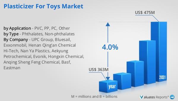
Plasticizer for Toys Market Share Driven by Stringent Safety Regulations and Shi …
Plasticizer for Toys Market Size
The global market for Plasticizer for Toys was valued at US$ 363 million in the year 2024 and is projected to reach a revised size of US$ 475 million by 2031, growing at a CAGR of 4.0% during the forecast period.
View sample report
https://reports.valuates.com/request/sample/QYRE-Auto-20U18169/Global_Plasticizer_for_Toys_Market_Research_Report_2024
The Plasticizer for Toys Market is witnessing steady market growth driven by increasing safety regulations and rising demand for non-toxic, child-safe materials. Plasticizers are…

Global Memory Interface Chip Market Intelligence: US$ 3.6 Billion Projection by …
Memory Interface Chip Market Size
The global Memory Interface Chip revenue was US$ 641.4 million in 2022 and is forecast to a readjusted size of US$ 3,612.7 million by 2029, growing at an impressive CAGR of 28.5% during the forecast period (2023-2029).
Get Free Sample: https://reports.valuates.com/request/sample/QYRE-Auto-19X16265/Global_and_India_Memory_Interface_Chip_Market_Report_Forecast_2023_2029
Major Trends
• Transition to 6400+ MT/s Speeds: The industry is rapidly standardizing higher speed tiers, pushing the limits of traditional RCD and Data Buffer designs.
• AI-Optimized Data Buffering: Manufacturers…

Global High Speed Memory Interface Chip Market Set for Resilient Growth, Project …
High Speed Memory Interface Chip Market Size
The global market for semiconductor was estimated at US$ 579 billion in the year 2022 and is projected to reach US$ 790 billion by 2029, growing at a CAGR of 6% during the forecast period.
Get Free Sample: https://reports.valuates.com/request/sample/QYRE-Auto-2X14355/Global_High_Speed_Memory_Interface_Chip_Market_Research_Report_2023
Major Trends
• Transition to DDR5-6400+: The industry is rapidly standardizing higher speed tiers, pushing the physical limits of traditional RCD and DB designs.
• AI-Centric Memory Architecture: Hyperscalers are adopting…
Global EV Memory Market Acceleration: US$ 4.45 Billion Projection by 2030, Fuele …
EV Memory Market Size
The global EV Memory market was valued at US$ 603 million in 2023 and is anticipated to reach US$ 4,453 million by 2030, witnessing an unprecedented CAGR of 31.7% during the forecast period 2024-2030.
• Growth Drivers by Segment: The DRAM segment is emerging as the largest contributor to market value, driven by the massive throughput required for on-vehicle AI inference in ADAS. In terms of application, the Vehicle…
More Releases for Inspection
Inspection Drones Market 2032: Advancements, Trends, and AI-Enabled Industrial I …
The Inspection Drones Market size was valued at USD 8.90 Billion in 2024 and the total Inspection Drones revenue is expected to grow at a CAGR of 12.9% from 2025 to 2032, reaching nearly USD 23.50 Billion.
Inspection Drones Market Overview:
The Inspection Drones Market has garnered strong attention from industries that require rapid and accurate evaluation of assets such as power lines, wind turbines, pipelines, bridges, and industrial installations. These drones…
Railway Inspection Services Market Outlook : Solutions, Inspection Vehicles & Sy …
Railway inspection is the practice of examining rail tracks for flaws that lead to catastrophic failures causing accidents. According to the U.S. Federal Railroad Administration Office of Safety Analysis, track defects are the second cause of railway accidents in U.S. Some of the reasons causing track defects are shear stresses, wheel/rail contact stresses, thermal stresses, residual stresses, and dynamic effects. Moreover, due to contact stresses defects such as tongue lipping,…
Surface Inspection Market: Surface Inspection Market to Grow to USD 10.29B by 20 …
Surface Inspection Market Scope:
Key Insights : Surface Inspection Market size was valued at USD 5.02 billion in 2022 and is poised to grow from USD 5.44 billion in 2023 to USD 10.29 billion by 2031, growing at a CAGR of 8.3% in the forecast period (2024-2031).
Discover Your Competitive Edge with a Free Sample Report :https://www.skyquestt.com/sample-request/surface-inspection-market
Access the full 2024 Market report for a comprehensive understanding @https://www.skyquestt.com/report/surface-inspection-market
In-Depth Exploration of the global…
Thermal Drone Inspection Market Soars as Industries Embrace Efficient and Safe I …
The global thermal drone inspection market is estimated to exceed US$ 282.4 million by the end of 2023, by growing at an impressive CAGR of 13.4% over the assessment period of 2023-2033.
The deployment of thermal cameras with infrared sensors and high quality image processors has significantly expanded the applications of the thermal drones. They can be utilized in various industries, for instance, firefighting, search & rescue, ariel utility and advanced…
beXel launched different inspection modules to improve inspection quality
beXel launched a Variety of modules to facilitate the inspection process and provide smart solutions for the customers such as
(Drops Inspection, Job order management, Lifting Inspection, NDT inspection, Tubular Inspection, Desktop Offline App).
A quality inspection involves measuring, examining, testing, or gauging various characteristics of a product and comparing those results with specified requirements to determine whether there is conformity.
Quality Control (QC) is critical to build and deliver products that meet…
Carlsbad, CA Mold Inspection and Asbestos Testing Services Offered by Murrieta M …
Carlsbad, CA, December 16, 2019 – EZ Mold Inspections continues expanding its service area in San Diego County and now provides asbestos testing and mold inspections in Carlsbad, California. The inspection company is based in the Murrieta-Temecula area. The company now serves nine areas in Riverside County and two cities in San Diego County including Oceanside, CA and Carlsbad, CA.
With more than two decades of experience in real estate and…
