Press release
Europe 3D Semiconductor Packaging Market Size 2025 Emerging Technologies, Opportunity and Forecast to 2032
3D Semiconductor Packaging Market
The 3D semiconductor packaging market is experiencing a period of rapid expansion, fueled by the relentless demand for smaller, faster, and more power-efficient electronic devices. This growth is driven by several key factors, including the increasing complexity of integrated circuits, the need for higher bandwidth and memory capacity, and the proliferation of advanced technologies such as artificial intelligence (AI), 5G, and the Internet of Things (IoT). Technological advancements in materials science, manufacturing processes, and design methodologies are enabling the development of innovative 3D packaging solutions that overcome the limitations of traditional 2D packaging. These advancements include Through Silicon Via (TSV) technology, which allows for vertical stacking of dies, Package-on-Package (PoP) technology, which enables the integration of multiple chips within a single package, and Fan-Out based technologies that provide increased I/O density and improved thermal performance. The 3D semiconductor packaging market plays a critical role in addressing global challenges by enabling the development of more energy-efficient and high-performance electronic devices that are essential for a wide range of applications, from mobile computing to automotive electronics to aerospace and defense. This is not just about shrinking devices, it is about enabling capabilities that simply were not possible before.
Get the full PDF sample copy of the report: (TOC, Tables and figures, and Graphs) https://www.consegicbusinessintelligence.com/request-sample/1326
Market Size:
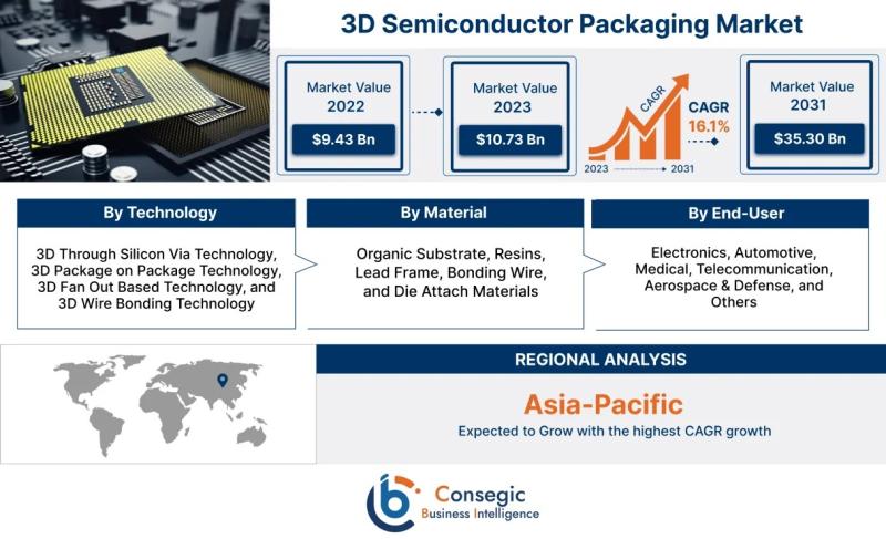
The 3D Semiconductor Packaging Market size is estimated to reach over USD 35.30 Billion by 2031 from a value of USD 9.43 Billion in 2022 and is projected to grow by USD 10.73 Billion in 2023, growing at a CAGR of 16.1% from 2023 to 2031.
Definition of Market:
The 3D Semiconductor Packaging Market encompasses the technologies, processes, and materials used to vertically stack and interconnect multiple semiconductor dies within a single package. This advanced packaging approach enables higher integration density, improved electrical performance, and reduced footprint compared to traditional 2D packaging methods. Key components within this market include:
Products: This includes the 3D packaged semiconductor devices themselves, such as memory chips, processors, and application-specific integrated circuits (ASICs).
Services: This includes design, manufacturing, assembly, and testing services related to 3D semiconductor packaging.
Systems: This refers to the equipment and tools used in the 3D packaging process, such as TSV etching and filling equipment, bonding machines, and inspection systems.
Key terms related to the market include:
Through Silicon Via (TSV): A vertical interconnect that passes through a silicon die, enabling vertical stacking of dies.
Package-on-Package (PoP): A packaging technology that stacks multiple packaged dies on top of each other.
Fan-Out Packaging: A packaging technology that redistributes the I/O connections of a die to a larger area, enabling higher I/O density.
Wafer-Level Packaging (WLP): Packaging that is performed at the wafer level before the individual dies are singulated.
Interposer: An intermediate substrate that is used to connect multiple dies within a package.
Get Discount On Report @ https://www.consegicbusinessintelligence.com/request-discount/1326
Market Scope and Overview:
The scope of the 3D Semiconductor Packaging Market encompasses a wide range of technologies, applications, and industries. The core technologies include Through Silicon Via (TSV), Package-on-Package (PoP), Fan-Out based technologies, and Wire Bonding technologies. These technologies are employed in various applications, including high-performance computing, memory, mobile devices, automotive electronics, medical devices, telecommunications infrastructure, and aerospace & defense systems. The industries served by this market include semiconductor manufacturers, electronics manufacturers, automotive suppliers, medical device companies, telecommunications equipment providers, and aerospace & defense contractors.
The 3D Semiconductor Packaging Market is crucial in the larger context of global trends such as the increasing demand for high-performance computing, the proliferation of mobile devices, and the growing importance of the Internet of Things (IoT). As electronic devices become more complex and require more processing power and memory capacity, 3D packaging offers a way to overcome the limitations of traditional 2D packaging. Furthermore, the increasing emphasis on energy efficiency and miniaturization is driving the adoption of 3D packaging solutions, which enable smaller, lighter, and more power-efficient devices. The demand for advanced packaging solutions is also fueled by the growth of emerging technologies such as artificial intelligence (AI), 5G, and autonomous vehicles, which require high-bandwidth and low-latency communication.
Market Segmentation:
The 3D Semiconductor Packaging Market can be segmented based on technology, material, and end-user. By technology, the market includes 3D Through Silicon Via (TSV) Technology, enabling vertical stacking of dies for enhanced performance; 3D Package on Package (PoP) Technology, allowing integration of multiple chips in a single package; 3D Fan-Out Based Technology, providing higher I/O density and improved thermal performance; and 3D Wire Bonding Technology, a traditional method adapted for 3D stacking. By material, the market is segmented into Organic Substrates, offering cost-effective solutions; Resins, providing insulation and protection; Lead Frames, providing electrical connections; Bonding Wire, used for die-to-package connections; and Die Attach Materials, ensuring secure die placement. By end-user, the market includes Electronics, benefiting from miniaturization and performance enhancements; Automotive, driven by ADAS and electric vehicle applications; Medical, requiring reliable and compact solutions; Telecommunication, driven by 5G infrastructure; Aerospace & Defense, demanding high-reliability and performance; and Others, encompassing various niche applications. Each segment contributes uniquely to the overall market growth, driven by specific application requirements and technological advancements.
Market Drivers:
Technological Advancements: Continuous advancements in 3D packaging technologies, such as TSV, PoP, and Fan-Out, are driving market growth by enabling higher integration density, improved electrical performance, and reduced footprint.
Increasing Demand for Miniaturization: The relentless demand for smaller and more portable electronic devices is driving the adoption of 3D packaging solutions, which enable higher integration density in a smaller form factor.
Growing Need for High Bandwidth and Memory Capacity: The increasing complexity of applications such as AI, 5G, and high-performance computing is driving the demand for high-bandwidth and memory capacity, which can be achieved through 3D packaging.
Proliferation of Advanced Technologies: The widespread adoption of advanced technologies such as AI, 5G, IoT, and autonomous vehicles is driving the demand for advanced semiconductor packaging solutions that can meet the stringent performance and reliability requirements of these applications.
Government Policies and Investments: Government initiatives and investments in research and development are supporting the growth of the 3D semiconductor packaging market by promoting innovation and technological advancements.
Market Key Trends:
Heterogeneous Integration: The integration of different types of chips (e.g., logic, memory, sensors) within a single package is becoming increasingly important to improve system performance and functionality.
Chiplet Design: The use of chiplets, which are small, modular chips that can be interconnected to create larger and more complex systems, is gaining traction as a way to reduce design complexity and improve time-to-market.
Advanced Materials: The development and adoption of new materials, such as advanced polymers and ceramics, are enabling the creation of more robust and reliable 3D packages.
Increasing Adoption of Fan-Out Packaging: Fan-out packaging is becoming increasingly popular due to its ability to provide higher I/O density and improved thermal performance.
Focus on Energy Efficiency: The growing emphasis on energy efficiency is driving the development of 3D packaging solutions that can reduce power consumption.
Market Opportunities:
Growth in AI and High-Performance Computing: The increasing demand for AI and high-performance computing applications is creating significant growth opportunities for 3D semiconductor packaging, which can enable the development of more powerful and efficient computing systems.
Expansion of 5G Infrastructure: The deployment of 5G infrastructure is driving the demand for advanced semiconductor packaging solutions that can support the high bandwidth and low latency requirements of 5G networks.
Adoption in Automotive Electronics: The increasing use of electronics in automobiles, particularly in advanced driver-assistance systems (ADAS) and electric vehicles (EVs), is creating growth opportunities for 3D semiconductor packaging, which can enable the development of more compact and reliable automotive electronics systems.
Innovations in Materials and Processes: Further innovation in areas like temporary bonding adhesives, new dielectrics, and advanced etching techniques.
Development of Standardized Chiplet Interfaces: The standardization of chiplet interfaces will facilitate the adoption of chiplet-based designs and create new opportunities for 3D semiconductor packaging.
Market Restraints:
High Initial Costs: The high initial costs associated with 3D packaging technologies, such as TSV manufacturing and advanced assembly equipment, can be a barrier to entry for smaller companies.
Technical Challenges: The development and manufacturing of 3D packages can be technically challenging, requiring specialized expertise and equipment.
Limited Standardization: The lack of standardization in 3D packaging technologies and processes can hinder the adoption of these technologies.
Thermal Management Issues: Managing heat dissipation in 3D packages can be challenging due to the high density of components.
Supply Chain Complexity: The 3D semiconductor packaging supply chain can be complex, involving multiple vendors and processes, which can increase costs and lead times.
Market Challenges:
The 3D semiconductor packaging market faces several critical challenges that could potentially hinder its growth trajectory. One of the most significant challenges is the high initial investment costs associated with advanced 3D packaging technologies. Implementing TSV (Through Silicon Via) and other advanced techniques requires sophisticated equipment and specialized processes, making it difficult for smaller players to enter the market. This can create a barrier to innovation and slow down the overall adoption rate, particularly in cost-sensitive applications.
Another major challenge is related to thermal management. As devices become more densely packed in 3D configurations, managing heat dissipation becomes increasingly complex. Inadequate thermal management can lead to performance degradation, reduced reliability, and even catastrophic failures. Developing effective cooling solutions, such as advanced heat sinks or liquid cooling systems, is crucial but adds complexity and cost to the packaging process.
Furthermore, the lack of standardization in 3D packaging technologies presents a significant hurdle. The absence of common standards can lead to interoperability issues, increased design complexity, and higher manufacturing costs. Encouraging industry-wide collaboration to establish standards is essential to drive widespread adoption and ensure seamless integration of 3D-packaged devices in various applications.
The complexity of the supply chain also poses a challenge. The 3D packaging process involves multiple steps and requires close coordination among different vendors, including die suppliers, packaging houses, and equipment manufacturers. Coordinating these disparate entities and ensuring timely delivery of high-quality components can be a logistical nightmare. Moreover, any disruptions in the supply chain, such as shortages of critical materials or equipment, can have a significant impact on production timelines and costs.
Finally, ensuring the reliability and quality of 3D-packaged devices is paramount. The intricate nature of 3D packaging introduces new failure modes that are not typically encountered in traditional 2D packaging. Rigorous testing and inspection procedures are essential to detect and eliminate defects, but these add to the overall cost and complexity of the manufacturing process. Meeting the stringent reliability requirements of demanding applications, such as automotive electronics and aerospace systems, requires continuous investment in quality control and process improvement.
Market Regional Analysis:
The 3D Semiconductor Packaging Market exhibits varying dynamics across different regions. Asia Pacific dominates the market due to the presence of major semiconductor manufacturers and electronics assembly hubs. Countries like Taiwan, South Korea, and China are key contributors, driven by strong government support and investments in advanced packaging technologies. North America holds a significant share, driven by the demand for high-performance computing and advanced electronics in industries like aerospace, defense, and telecommunications. The presence of leading semiconductor companies and research institutions in the region fosters innovation and technological advancements. Europe also holds a considerable market share, driven by the automotive and industrial sectors. The region's focus on energy efficiency and sustainability promotes the adoption of 3D packaging solutions. Each region's market dynamics are influenced by factors such as economic conditions, government policies, technological infrastructure, and industry-specific requirements.
Frequently Asked Questions:
What are the growth projections for the 3D Semiconductor Packaging Market? The market is projected to grow at a CAGR of 16.1% from 2023 to 2031, reaching over USD 35.30 Billion by 2031.
What are the key trends in the 3D Semiconductor Packaging Market?
Key trends include heterogeneous integration, chiplet design, advanced materials, increasing adoption of Fan-Out packaging, and a focus on energy efficiency.
What are the most popular Market types in 3D Semiconductor Packaging?
3D Through Silicon Via (TSV) Technology and 3D Package on Package (PoP) Technology are currently the most popular market types, driven by their ability to enable high integration density and improved performance.
Our Other Pages
https://www.linkedin.com/company/indepth-business-solutions/
https://www.linkedin.com/company/deeptech-insights/
https://www.linkedin.com/company/techforward-trends/
https://www.linkedin.com/company/momentum-marketing-group24/
https://www.linkedin.com/company/tech-savvy-innovators/"
Contact Us:
Consegic Business intelligence Pvt Ltd
Baner Road, Baner, Pune, Maharashtra - 411045
+1-252-552-1404
info@consegicbusinessintelligence.com
sales@consegicbusinessintelligence.com
Web - https://www.consegicbusinessintelligence.com/
About Us:
Consegic Business Intelligence is a data measurement and analytics service provider that gives the most exhaustive and reliable analysis available of global consumers and markets. Our research and competitive landscape allow organizations to record competing evolutions and apply strategies accordingly to set up a rewarding benchmark in the market. We are an intellectual team of experts working together with the winning inspirations to create and validate actionable insights that ensure business growth and profitable outcomes.
We provide an exact data interpretation and sources to help clients around the world understand current market scenarios and how to best act on these learnings. Our team provides on-the-ground data analysis, Portfolio Expansion, Quantitative and qualitative analysis, Telephone Surveys, Online Surveys, and Ethnographic studies. Moreover, our research reports provide market entry plans, market feasibility and opportunities, economic models, analysis, and an advanced plan of action with consulting solutions. Our consumerization gives all-inclusive end-to-end customer insights for agile, smarter, and better decisions to help business expansion.
Connect with us on:
LinkedIn - https://www.linkedin.com/company/consegic-business-intelligence/
YouTube - https://www.youtube.com/@ConsegicBusinessIntelligence22
Facebook - https://www.facebook.com/profile.php?id=61575657487319
X - https://x.com/Consegic_BI
Instagram - https://www.instagram.com/cbi._insights/
This release was published on openPR.
Permanent link to this press release:
Copy
Please set a link in the press area of your homepage to this press release on openPR. openPR disclaims liability for any content contained in this release.
You can edit or delete your press release Europe 3D Semiconductor Packaging Market Size 2025 Emerging Technologies, Opportunity and Forecast to 2032 here
News-ID: 4096272 • Views: …
More Releases from Consegic Business Intelligence Pvt. Ltd
Europe Pharmaceutical Manufacturing Equipment Market 2025 Industry Updates, Futu …
Introduction:
The Pharmaceutical Manufacturing Equipment Market is experiencing robust growth, driven by a confluence of factors reshaping the landscape of pharmaceutical production. Increasing global demand for pharmaceuticals, fueled by an aging population and the rise of chronic diseases, necessitates advanced and efficient manufacturing processes. Technological advancements, such as continuous manufacturing, automation, and digitalization, are revolutionizing traditional methods, improving production efficiency, reducing costs, and enhancing product quality. Stringent regulatory requirements and the…
Europe Vibration Damping Materials Market Size 2025 Overview, Manufacturers, Typ …
Introduction:
The Vibration Damping Materials market is experiencing significant growth, driven by the increasing demand for noise and vibration reduction across various industries. Key drivers include stringent environmental regulations, the growing automotive industry, particularly the electric vehicle (EV) sector, and the need for enhanced comfort and safety in residential and commercial buildings. Technological advancements in materials science are also playing a pivotal role, with the development of more efficient and durable…
Europe Lightweight Aggregates Market Size 2025 Emerging Technologies, Opportunit …
Introduction:
The Lightweight Aggregates Market is experiencing substantial growth driven by several key factors. Primarily, the increasing demand for sustainable and eco-friendly construction materials is fueling the adoption of lightweight aggregates. These materials offer superior insulation properties, reduced transportation costs, and contribute to the overall reduction of the carbon footprint of construction projects. Technological advancements in the production and application of lightweight aggregates are also playing a crucial role, enhancing their…
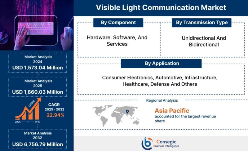
Europe Visible Light Communication Market Share, Growth, Size, Industry Trends, …
Introduction:
The Visible Light Communication (VLC) market is experiencing significant growth, driven by the increasing demand for faster, more secure, and energy-efficient communication technologies. VLC leverages light waves for data transmission, offering a complementary solution to traditional radio frequency (RF) based wireless communication. Key drivers include the proliferation of LED lighting, growing concerns about RF spectrum congestion, and the need for secure communication in sensitive environments. Technological advancements, such as improved…
More Releases for Packaging
Personalized Packaging Market 2019 By Key Players: Owens Illinois, Salazar Packa …
Personalized Packaging Market research report delivers a close watch on leading competitors with strategic analysis, micro and macro market trend and scenarios, pricing analysis and a holistic overview of the market situations in the forecast period.
Download PDF Sample of this Report @
http://www.supplydemandmarketresearch.com/home/contact/277379?ref=Sample-and-Brochure&toccode=SDMRCH277379&utm_source=S2
The following manufacturers are covered:
Owens Illinois
Salazar Packaging
Design Packaging
PrimeLine Packaging
International Packaging
Elegant Packaging
Pak Factory
ABOX Packaging
ACG Ecopak
CB Group
SoOPAK Company
Huhtamaki…
E-Commerce Packaging Market by Top Key Players - Pioneer Packaging, Arihant pack …
E-commerce packaging involves the use of materials for safe packaging of products sold by the e-commerce industry. E-commerce packaging plays a vital role in the consumers' perception about the e-retailer. It also indicates the perceived value of the item received. Packaging reflects the value of shipment in the e-commerce supply chain, that is, better the packaging, better the product inside it.
Get Sample Copy of this Report @ https://www.bigmarketresearch.com/request-sample/2904563
The E-Commerce…
Luxury Packaging Market 2019 SWOT Analysis By Top Key Players; MW Luxury Packagi …
Luxury Packaging Market report provides an in-depth overview of product specification, technology, product type and production analysis considering major factors such as revenue, cost, gross and gross margin. The company profiles of all the key players and brands that are dominating the Luxury Packaging Market with moves like product launches, joint ventures, merges and accusations which in turn is affecting the sales, import, export, revenue and CAGR values are mentioned…
Global Luxury Packaging Market 2019 Top Key Players: MW Luxury Packaging, Progre …
Summary
WiseGuyReports.com adds “Luxury Packaging Market 2019 Global Analysis, Growth, Trends and Opportunities Research Report Forecasting to 2024” reports to its database.
This report provides in depth study of “Luxury Packaging Market” using SWOT analysis i.e. Strength, Weakness, Opportunities and Threat to the organization. The Luxury Packaging Market report also provides an in-depth survey of key players in the market which is based on the various objectives of an organization such as…
Top Manufacturer in Luxury Packaging Market 2019: MW Luxury Packaging, Progress …
Luxury packaging is used for packaging and decorating high-end products.An increase in the luxury product consumption rate and the number of product launches in the fashion and cosmetic sectors are some major factors driving the market growth.
The global Luxury Packaging market is valued at xx million US$ in 2018 and will reach xx million US$ by the end of 2025, growing at a CAGR of xx% during 2019-2025. The objectives…
Personalized Packaging Market 2025 | Design Packaging, Inc., PrimeLine Packaging …
As per the new market report published by Research Report Insights titled ‘Personalized Packaging Market’: Global Industry Analysis and Forecast 2017-2025’, global personalized packaging market attained a value worth US$ 25,577.9 Mn in 2017 and will possibly thrive at a promising CAGR of 5.1% over the forecast period (2017-2025). The global personalized packaging market has witnessed solid growth during the past few decades, owing to the increasing trend of luxury…
