Press release
Semiconductor Inspection System Market Insights: Emerging Opportunities, Size Estimation & Forecast to 2032
semiconductor inspection system market
The Semiconductor Inspection System market is a critical component of the global semiconductor industry, playing a pivotal role in ensuring the quality, reliability, and performance of integrated circuits. This market is experiencing robust growth driven by several key factors, including the increasing complexity of semiconductor devices, the growing demand for advanced electronics in various sectors such as consumer electronics, automotive, healthcare, and industrial automation, and the relentless pursuit of miniaturization and higher performance. Technological advancements, particularly in areas like advanced lithography, 3D packaging, and novel materials, are pushing the boundaries of manufacturing processes, necessitating sophisticated inspection systems capable of detecting increasingly smaller defects. Furthermore, government initiatives and investments aimed at bolstering domestic semiconductor manufacturing capabilities are also contributing to market expansion. As the global demand for semiconductors continues to surge, fueled by trends such as artificial intelligence, 5G connectivity, and the Internet of Things (IoT), the semiconductor inspection system market is poised to play an increasingly crucial role in addressing the global challenge of ensuring a stable and reliable supply of high-quality semiconductors.
Get the full PDF sample copy of the report: (TOC, Tables and figures, and Graphs) https://www.consegicbusinessintelligence.com/request-sample/1250
Market Size:
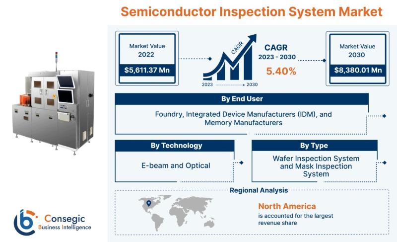
The Semiconductor Inspection System market size is estimated to reach over USD 8,380.01 Million by 2030 from a value of USD 5,611.37 Million in 2022, growing at a CAGR of 5.40% from 2023 to 2030.
Definition of Market:
The Semiconductor Inspection System market encompasses the range of equipment, software, and services used to detect, analyze, and classify defects in semiconductor wafers, masks, and packaged devices. These systems are integral to the manufacturing process, ensuring that only high-quality chips reach the market. The market includes automated optical inspection (AOI) systems, e-beam inspection tools, and other advanced technologies. Key terms within this market include:
Wafer Inspection: The process of examining semiconductor wafers for defects at various stages of production.
Mask Inspection: The inspection of photomasks (or reticles), which are used in the lithography process to pattern circuit designs onto wafers.
Defect Detection: The identification of imperfections, contaminants, or structural anomalies on semiconductor materials.
Metrology: The science of measurement, essential for characterizing the size, shape, and composition of defects.
Yield Management: Strategies and techniques to maximize the number of functional chips produced from each wafer.
Automatic Defect Classification (ADC): Software that automatically categorizes defects based on their characteristics, facilitating efficient analysis and correction.
These systems are used by foundries, integrated device manufacturers (IDMs), and memory manufacturers to improve yield, reduce manufacturing costs, and enhance the performance and reliability of semiconductor devices. The effectiveness of inspection systems directly impacts the profitability and competitiveness of semiconductor manufacturers.
Get Discount On Report @ https://www.consegicbusinessintelligence.com/request-discount/1250
Market Scope and Overview:
The scope of the Semiconductor Inspection System market is broad, encompassing various technologies, applications, and industries. From a technological standpoint, the market includes optical inspection, electron beam inspection, and atomic force microscopy (AFM), among others. These technologies are deployed across various stages of semiconductor manufacturing, from wafer fabrication to packaging and testing. The applications of these systems range from defect detection and metrology to process control and yield management. The industries served by this market are diverse, including semiconductor foundries, integrated device manufacturers (IDMs), memory manufacturers, and outsourced semiconductor assembly and test (OSAT) providers. The market also extends to suppliers of inspection equipment, software, and related services.
The semiconductor inspection system market's importance is highlighted within the larger context of global technological trends. The increasing demand for semiconductors in emerging technologies like artificial intelligence, 5G, and the Internet of Things (IoT) is driving the need for more advanced and reliable inspection systems. Moreover, the complexity of modern semiconductor devices, characterized by shrinking feature sizes and intricate 3D architectures, necessitates sophisticated inspection capabilities. This market is essential for ensuring the quality and reliability of these advanced semiconductors, enabling the continued progress of these key technological trends. As semiconductor manufacturers strive to improve yield and reduce costs, the semiconductor inspection system market will remain a critical enabler, facilitating the development and production of next-generation electronic devices.
Top Key Players in this Market
ViSCO Technologies USA, Inc., TAKANO CO., LTD., UENO SEIKI CO., LTD., Nikon Metrology NV., Toray Engineering (TASMIT, Inc.), Onto Innovation, Inc., C&D Semiconductor Services Inc., Lasertec Corporation, KLA Corporation, Applied Materials Inc., Hitachi Group, ASML Holding N.V., and JEOL Ltd.
Market Segmentation:
The Semiconductor Inspection System market can be segmented by:
By Type: Wafer Inspection System and Mask Inspection System. Wafer inspection systems are used to detect defects on semiconductor wafers during the manufacturing process, while mask inspection systems are used to ensure the quality of photomasks used in lithography.
By Technology: E-beam and Optical. E-beam inspection systems use electron beams to detect defects, offering high resolution but slower throughput. Optical inspection systems use light to detect defects, providing faster throughput but lower resolution.
By End User: Foundry, Integrated Device Manufacturers (IDM), and Memory Manufacturers. Foundries manufacture chips for other companies, IDMs design and manufacture their own chips, and memory manufacturers specialize in producing memory chips. Each end-user segment has unique inspection requirements based on their specific manufacturing processes and products.
Market Drivers:
Technological Advancements: The continuous development of smaller, more complex semiconductor devices necessitates advanced inspection systems capable of detecting increasingly smaller defects.
Increasing Demand for High-Quality Semiconductors: The growing demand for semiconductors in various applications, such as consumer electronics, automotive, and industrial automation, is driving the need for high-quality, reliable chips, which in turn drives the demand for advanced inspection systems.
Government Policies and Initiatives: Government support for domestic semiconductor manufacturing, including incentives for research and development, is boosting investment in inspection equipment.
Need for Improved Yield and Reduced Costs: Semiconductor manufacturers are constantly seeking ways to improve yield and reduce costs, and advanced inspection systems play a crucial role in achieving these goals.
Market Key Trends:
Adoption of Artificial Intelligence (AI) and Machine Learning (ML): AI and ML algorithms are increasingly being integrated into inspection systems to improve defect detection accuracy, automate defect classification, and enhance process control.
Increasing Use of 3D Inspection Techniques: As semiconductor devices become more three-dimensional, there is a growing need for inspection systems that can provide accurate 3D measurements of defects.
Growing Focus on Advanced Packaging Inspection: Advanced packaging technologies, such as 2.5D and 3D packaging, are becoming increasingly important, and inspection systems are needed to ensure the quality and reliability of these packages.
Shift Towards More Integrated Inspection Solutions: Semiconductor manufacturers are seeking more integrated inspection solutions that combine multiple inspection techniques into a single platform.
Market Opportunities:
Growth in Advanced Packaging Inspection: The increasing adoption of advanced packaging technologies presents a significant growth opportunity for inspection system vendors.
Expansion into New Applications: The semiconductor inspection system market can expand into new applications, such as the inspection of microLED displays and power devices.
Development of More Affordable Inspection Systems: There is a need for more affordable inspection systems that can be used by smaller semiconductor manufacturers and research institutions.
Innovations in Defect Detection Algorithms: Continued innovation in defect detection algorithms, particularly those based on AI and ML, can lead to significant improvements in inspection system performance.
Market Restraints:
High Initial Costs: The high cost of advanced inspection systems can be a barrier to entry for smaller semiconductor manufacturers.
Complexity of Inspection Data: The vast amount of data generated by inspection systems can be challenging to manage and analyze.
Limited Availability of Skilled Personnel: The operation and maintenance of advanced inspection systems require skilled personnel, which can be in short supply.
Technological Challenges: Detecting increasingly smaller defects in advanced semiconductor devices requires overcoming significant technological challenges.
Market Challenges:
The Semiconductor Inspection System market faces a multitude of challenges stemming from the ever-evolving nature of the semiconductor industry. One of the foremost challenges is the relentless drive towards miniaturization, which demands inspection systems capable of detecting defects at increasingly smaller dimensions. As feature sizes shrink to the nanometer scale, the sensitivity and resolution of inspection equipment must continuously improve, necessitating substantial investments in research and development. This also translates into the need for more sophisticated algorithms and data processing techniques to accurately identify and classify defects from vast amounts of complex data. Moreover, the transition to more complex 3D chip architectures presents a significant challenge, as traditional 2D inspection methods are inadequate for characterizing the internal structures and interfaces of these devices.
Another significant challenge arises from the increasing diversity of materials and processes used in semiconductor manufacturing. New materials, such as high-k dielectrics and advanced metals, require inspection techniques tailored to their specific properties. Similarly, the proliferation of novel manufacturing processes, such as extreme ultraviolet (EUV) lithography and atomic layer deposition (ALD), necessitates inspection systems that can effectively monitor and control these processes. Furthermore, the growing emphasis on advanced packaging technologies, such as chiplets and heterogeneous integration, creates new inspection challenges related to the assembly and interconnect of multiple chips. These challenges demand that inspection system vendors develop highly adaptable and versatile solutions that can accommodate a wide range of materials, processes, and device architectures.
Beyond the technical challenges, the Semiconductor Inspection System market also faces economic and logistical hurdles. The high cost of advanced inspection equipment can be a significant barrier to entry for smaller semiconductor manufacturers and research institutions. Additionally, the complex installation and maintenance requirements of these systems necessitate skilled personnel, which can be in short supply. Furthermore, the global nature of the semiconductor supply chain creates logistical challenges related to the transportation, installation, and support of inspection equipment in various locations around the world. Addressing these challenges requires innovative business models, such as equipment leasing and remote support services, as well as investments in training and education programs to develop a skilled workforce. Overall, overcoming these multifaceted challenges is essential for ensuring the continued growth and innovation of the Semiconductor Inspection System market.
Market Regional Analysis:
The Semiconductor Inspection System market exhibits varying dynamics across different regions, driven by factors such as the concentration of semiconductor manufacturing facilities, government investments, and technological capabilities. Asia-Pacific (APAC) is the largest market due to the presence of major semiconductor foundries and integrated device manufacturers in countries like Taiwan, South Korea, and China. These countries are heavily investing in expanding their semiconductor manufacturing capacity, which in turn drives the demand for inspection systems. North America is also a significant market, driven by the presence of leading semiconductor equipment vendors and research institutions. The region is focused on developing advanced inspection technologies and maintaining its competitive edge in the semiconductor industry. Europe represents a smaller but growing market, with a focus on specialized applications such as automotive and industrial semiconductors. Government initiatives to strengthen the European semiconductor ecosystem are expected to further drive market growth in the region. Each region's market dynamics are influenced by its unique economic, technological, and political factors.
Frequently Asked Questions:
What is the projected growth rate of the Semiconductor Inspection System market?
The market is projected to grow at a CAGR of 5.40% from 2023 to 2030.
What are the key trends in this market?
Key trends include the adoption of AI and ML, increasing use of 3D inspection, and a growing focus on advanced packaging inspection.
Which are the most popular Market types?
Wafer Inspection System and Mask Inspection System
"
Contact Us:
Consegic Business intelligence Pvt Ltd
Baner Road, Baner, Pune, Maharashtra - 411045
(US) (505) 715-4344
info@consegicbusinessintelligence.com
sales@consegicbusinessintelligence.com
Web - https://www.consegicbusinessintelligence.com/
About Us:
Consegic Business Intelligence is a data measurement and analytics service provider that gives the most exhaustive and reliable analysis available of global consumers and markets. Our research and competitive landscape allow organizations to record competing evolutions and apply strategies accordingly to set up a rewarding benchmark in the market. We are an intellectual team of experts working together with the winning inspirations to create and validate actionable insights that ensure business growth and profitable outcomes.
We provide an exact data interpretation and sources to help clients around the world understand current market scenarios and how to best act on these learnings. Our team provides on-the-ground data analysis, Portfolio Expansion, Quantitative and qualitative analysis, Telephone Surveys, Online Surveys, and Ethnographic studies. Moreover, our research reports provide market entry plans, market feasibility and opportunities, economic models, analysis, and an advanced plan of action with consulting solutions. Our consumerization gives all-inclusive end-to-end customer insights for agile, smarter, and better decisions to help business expansion.
Connect with us on:
LinkedIn - https://www.linkedin.com/company/consegic-business-intelligence/
YouTube - https://www.youtube.com/@ConsegicBusinessIntelligence22
Facebook - https://www.facebook.com/profile.php?id=61575657487319
X - https://x.com/Consegic_BI
Instagram - https://www.instagram.com/cbi._insights/
This release was published on openPR.
Permanent link to this press release:
Copy
Please set a link in the press area of your homepage to this press release on openPR. openPR disclaims liability for any content contained in this release.
You can edit or delete your press release Semiconductor Inspection System Market Insights: Emerging Opportunities, Size Estimation & Forecast to 2032 here
News-ID: 4051880 • Views: …
More Releases from Consegic Business Intelligence Pvt. Ltd
Europe Pharmaceutical Manufacturing Equipment Market 2025 Industry Updates, Futu …
Introduction:
The Pharmaceutical Manufacturing Equipment Market is experiencing robust growth, driven by a confluence of factors reshaping the landscape of pharmaceutical production. Increasing global demand for pharmaceuticals, fueled by an aging population and the rise of chronic diseases, necessitates advanced and efficient manufacturing processes. Technological advancements, such as continuous manufacturing, automation, and digitalization, are revolutionizing traditional methods, improving production efficiency, reducing costs, and enhancing product quality. Stringent regulatory requirements and the…
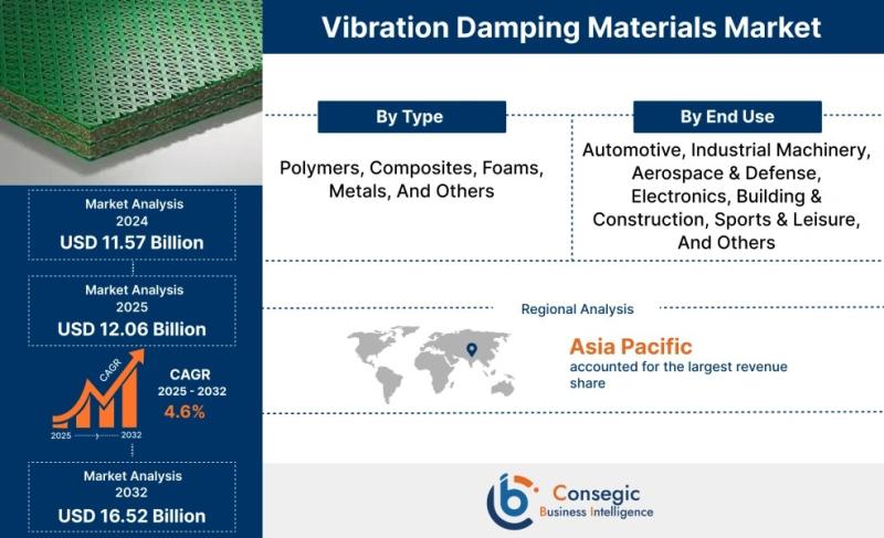
Europe Vibration Damping Materials Market Size 2025 Overview, Manufacturers, Typ …
Introduction:
The Vibration Damping Materials market is experiencing significant growth, driven by the increasing demand for noise and vibration reduction across various industries. Key drivers include stringent environmental regulations, the growing automotive industry, particularly the electric vehicle (EV) sector, and the need for enhanced comfort and safety in residential and commercial buildings. Technological advancements in materials science are also playing a pivotal role, with the development of more efficient and durable…
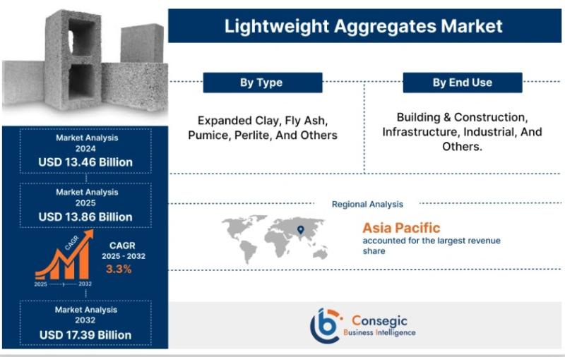
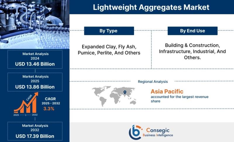
Europe Lightweight Aggregates Market Size 2025 Emerging Technologies, Opportunit …
Introduction:
The Lightweight Aggregates Market is experiencing substantial growth driven by several key factors. Primarily, the increasing demand for sustainable and eco-friendly construction materials is fueling the adoption of lightweight aggregates. These materials offer superior insulation properties, reduced transportation costs, and contribute to the overall reduction of the carbon footprint of construction projects. Technological advancements in the production and application of lightweight aggregates are also playing a crucial role, enhancing their…
Europe Visible Light Communication Market Share, Growth, Size, Industry Trends, …
Introduction:
The Visible Light Communication (VLC) market is experiencing significant growth, driven by the increasing demand for faster, more secure, and energy-efficient communication technologies. VLC leverages light waves for data transmission, offering a complementary solution to traditional radio frequency (RF) based wireless communication. Key drivers include the proliferation of LED lighting, growing concerns about RF spectrum congestion, and the need for secure communication in sensitive environments. Technological advancements, such as improved…
More Releases for Inspection
Inspection Drones Market 2032: Advancements, Trends, and AI-Enabled Industrial I …
The Inspection Drones Market size was valued at USD 8.90 Billion in 2024 and the total Inspection Drones revenue is expected to grow at a CAGR of 12.9% from 2025 to 2032, reaching nearly USD 23.50 Billion.
Inspection Drones Market Overview:
The Inspection Drones Market has garnered strong attention from industries that require rapid and accurate evaluation of assets such as power lines, wind turbines, pipelines, bridges, and industrial installations. These drones…
Railway Inspection Services Market Outlook : Solutions, Inspection Vehicles & Sy …
Railway inspection is the practice of examining rail tracks for flaws that lead to catastrophic failures causing accidents. According to the U.S. Federal Railroad Administration Office of Safety Analysis, track defects are the second cause of railway accidents in U.S. Some of the reasons causing track defects are shear stresses, wheel/rail contact stresses, thermal stresses, residual stresses, and dynamic effects. Moreover, due to contact stresses defects such as tongue lipping,…
Surface Inspection Market: Surface Inspection Market to Grow to USD 10.29B by 20 …
Surface Inspection Market Scope:
Key Insights : Surface Inspection Market size was valued at USD 5.02 billion in 2022 and is poised to grow from USD 5.44 billion in 2023 to USD 10.29 billion by 2031, growing at a CAGR of 8.3% in the forecast period (2024-2031).
Discover Your Competitive Edge with a Free Sample Report :https://www.skyquestt.com/sample-request/surface-inspection-market
Access the full 2024 Market report for a comprehensive understanding @https://www.skyquestt.com/report/surface-inspection-market
In-Depth Exploration of the global…
Thermal Drone Inspection Market Soars as Industries Embrace Efficient and Safe I …
The global thermal drone inspection market is estimated to exceed US$ 282.4 million by the end of 2023, by growing at an impressive CAGR of 13.4% over the assessment period of 2023-2033.
The deployment of thermal cameras with infrared sensors and high quality image processors has significantly expanded the applications of the thermal drones. They can be utilized in various industries, for instance, firefighting, search & rescue, ariel utility and advanced…
beXel launched different inspection modules to improve inspection quality
beXel launched a Variety of modules to facilitate the inspection process and provide smart solutions for the customers such as
(Drops Inspection, Job order management, Lifting Inspection, NDT inspection, Tubular Inspection, Desktop Offline App).
A quality inspection involves measuring, examining, testing, or gauging various characteristics of a product and comparing those results with specified requirements to determine whether there is conformity.
Quality Control (QC) is critical to build and deliver products that meet…
Carlsbad, CA Mold Inspection and Asbestos Testing Services Offered by Murrieta M …
Carlsbad, CA, December 16, 2019 – EZ Mold Inspections continues expanding its service area in San Diego County and now provides asbestos testing and mold inspections in Carlsbad, California. The inspection company is based in the Murrieta-Temecula area. The company now serves nine areas in Riverside County and two cities in San Diego County including Oceanside, CA and Carlsbad, CA.
With more than two decades of experience in real estate and…
