Press release
Global E-Beam Wafer Inspection System Market Poised for Exponential Growth, Expected to Reach US$ 6.1 Bn by 2031

E-Beam Wafer Inspection System Market
Download to explore critical insights from our Report in this sample - https://www.transparencymarketresearch.com/sample/sample.php?flag=S&rep_id=15884
Market Overview
E-beam wafer inspection systems are pivotal in modern semiconductor fabrication processes, leveraging high-energy electron beams to examine wafers for defects at extremely high resolutions. These systems provide the detailed insights necessary to maintain the integrity of complex semiconductor devices, including logic and memory chips, during and after the production process.
The increasing miniaturization of semiconductor components and the shift toward advanced technology nodes have elevated the demand for inspection tools that can detect defects invisible to conventional optical systems. The e-beam wafer inspection system market is thus becoming essential for quality control and yield optimization in semiconductor manufacturing.
Market Drivers & Trends
A key driver of market expansion is the adoption of Extreme Ultraviolet (EUV) lithography, which supports the development of next-generation chips at nodes below 10nm. The increasing complexity of integrated circuits, due to multi-layer stacking in 2.5D and 3D architectures, also necessitates high-resolution, high-throughput inspection tools.
One of the latest trends shaping the industry is the development of multi-beam inspection systems. These systems deliver significantly improved throughput and enable the detection of minute defects that are undetectable using traditional single-beam tools. As semiconductors become smaller and more complex, these multi-beam systems offer the scale and speed required for industrial-scale production.
Key Players and Industry Leaders
Several major industry players are leading innovation in this market, including:
Applied Materials Inc.
ASML Holding N.V.
Hitachi Ltd.
HOLON Co., Ltd.
KLA Corporation
MKS Instruments, Inc.
PDF Solutions
Photo electron Soul Inc.
TASMIT, Inc.
Telemark Factory
ZEISS Semiconductor Manufacturing Technology
These companies are focused on improving electron optical systems, enhancing data processing capabilities, and offering advanced analytics that facilitate defect detection and faster decision-making in semiconductor fabrication lines.
Recent Developments
Innovation remains central to competitive strategy in this market:
Hitachi introduced the GS1000 e-beam inspection system designed for EUV 3nm and 5nm processes. It combines high-resolution imaging with rapid data processing, tailored to meet the defect detection demands of cutting-edge semiconductor nodes.
KLA Corporation launched the eSL10TM e-beam defect inspection technology in 2020, aimed at reducing inspection times and improving yields for advanced memory and logic chips. The platform is especially effective for detecting anomalies in EUV-patterned wafers.
Latest Market Trends
The shift toward multi-beam inspection is the most notable trend, driven by the need for faster, more efficient analysis at scale. Traditional single-beam systems face throughput limitations that make them less suitable for high-volume manufacturing. Multi-beam technology is now becoming a cornerstone for semiconductor fabs aiming to maintain pace with innovation while ensuring yield optimization.
Additionally, the rise in automated defect classification and AI-powered analytics in e-beam systems is enhancing their role in predictive maintenance and process improvement, providing fab operators with better insights and faster root cause analysis.
Market Opportunities
Opportunities abound in the areas of:
Advanced nodes (7nm and below) where inspection precision is critical
2.5D and 3D packaging technologies, which demand defect detection across multiple layers and interfaces
AI-integrated inspection platforms offering real-time analysis and feedback loops for yield improvement
Furthermore, emerging markets in automotive electronics, healthcare devices, and IoT present untapped demand for semiconductor components, thus requiring inspection technologies to ensure quality and reliability at high volumes.
Future Outlook
Looking ahead, the e-beam wafer inspection system market will continue to grow rapidly as semiconductor technologies evolve toward smaller nodes and more complex structures. The deployment of 5G, AI, and autonomous vehicles will further drive the need for defect-free chips with high reliability.
Analysts forecast a growing preference for multi-beam systems, AI-enhanced analytics, and integration with smart manufacturing platforms. Vendors investing in R&D and strategic partnerships will be best positioned to capitalize on this market's exponential growth potential.
Buy this Premium Research Report to stay ahead with cutting-edge data - https://www.transparencymarketresearch.com/checkout.php?rep_id=15884
About Transparency Market Research
Transparency Market Research, a global market research company registered at Wilmington, Delaware, United States, provides custom research and consulting services. Our exclusive blend of quantitative forecasting and trends analysis provides forward-looking insights for thousands of decision makers. Our experienced team of Analysts, Researchers, and Consultants use proprietary data sources and various tools & techniques to gather and analyses information.
Our data repository is continuously updated and revised by a team of research experts, so that it always reflects the latest trends and information. With a broad research and analysis capability, Transparency Market Research employs rigorous primary and secondary research techniques in developing distinctive data sets and research material for business reports.
Contact:
Transparency Market Research Inc.
CORPORATE HEADQUARTER DOWNTOWN,
1000 N. West Street,
Suite 1200, Wilmington, Delaware 19801 USA
Tel: +1-518-618-1030
USA - Canada Toll Free: 866-552-3453
Website: https://www.transparencymarketresearch.com
Email: sales@transparencymarketresearch.com
This release was published on openPR.
Permanent link to this press release:
Copy
Please set a link in the press area of your homepage to this press release on openPR. openPR disclaims liability for any content contained in this release.
You can edit or delete your press release Global E-Beam Wafer Inspection System Market Poised for Exponential Growth, Expected to Reach US$ 6.1 Bn by 2031 here
News-ID: 4001937 • Views: …
More Releases from Transparency Market Research
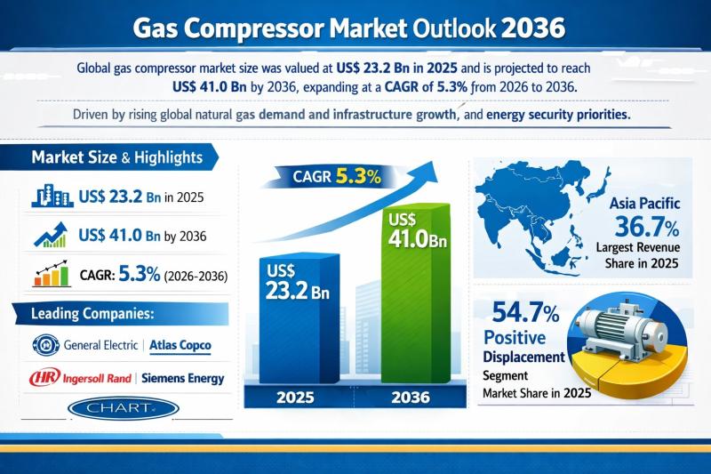
Gas Compressor Market Outlook 2036: Global Industry Expected to Reach US$ 41.0 B …
The global gas compressor market was valued at US$ 23.2 Bn in 2025 and is projected to reach US$ 41.0 Bn by 2036, expanding at a compound annual growth rate (CAGR) of 5.3% from 2026 to 2036. This steady growth trajectory reflects the structural importance of gas compression systems across upstream, midstream, and downstream gas value chains. Rising natural gas consumption, expansion of pipeline and LNG infrastructure, and national energy…

Anesthesia Drugs Market to be Worth USD 12.6 Bn by 2036 - By Drug / By Applicati …
The global anesthesia drugs market was valued at US$ 7.6 billion in 2025 and is projected to reach US$ 12.6 billion by 2036, expanding at a compound annual growth rate (CAGR) of 4.7% from 2026 to 2036. This steady growth trajectory reflects the essential and non-substitutable role of anesthesia drugs in modern healthcare systems. As surgical interventions continue to rise globally-across both elective and emergency procedures-the demand for safe, effective,…
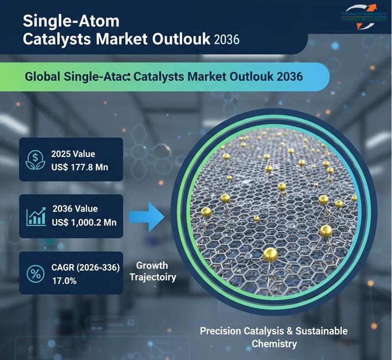
Single-Atom Catalysts Market Size is Expected to Expand from US$ 177.8 Million t …
The global single-atom catalysts (SACs) market is poised for remarkable growth as industries seek highly efficient, cost-effective, and sustainable catalytic solutions. Valued at US$ 177.8 million in 2025, the market is projected to reach US$ 1,000.2 million by 2036, expanding at a robust compound annual growth rate (CAGR) of 17.0% from 2026 to 2036. This rapid expansion reflects the growing importance of advanced catalysis in energy, chemicals, environmental protection, and…

Non-specific Endonuclease Market to Reach USD 726.6 Million by 2036, Supported b …
The non-specific endonuclease market is witnessing steady growth, driven by the expanding use of molecular biology tools across biotechnology, pharmaceuticals, diagnostics, and academic research. Non-specific endonucleases are enzymes that cleave nucleic acids without requiring a specific recognition sequence, making them highly valuable for applications such as DNA/RNA degradation, sample preparation, viscosity reduction, and contamination control. Their broad activity profile differentiates them from restriction enzymes and enables versatile usage across multiple…
More Releases for Wafer
Semiconductor Silicon Wafer Market Is Going to Boom |• Silicon Wafer • Globa …
Worldwide Market Reports has released a new in-depth research study on the "Semiconductor Silicon Wafer Market," highlighting strong growth potential in the coming years. The report delivers a structured and data-driven analysis of the market landscape, combining robust research methodology, market sizing, validated data modeling, and insights sourced from reliable primary and secondary channels.
The study thoroughly examines key market aspects, including growth drivers, restraints, challenges, emerging opportunities, technological advancements, innovation…
Semiconductor Wafer Electrostatic Chucks for 300mm Wafer Market Size, Trends & F …
Semiconductor Wafer Electrostatic Chucks for 300mm Wafer Market Size
The global Semiconductor Wafer Electrostatic Chucks for 300mm Wafer market is projected to grow from US$ 1227 million in 2024 to US$ 1672.7 million by 2030, at a Compound Annual Growth Rate (CAGR) of 5.3% during the forecast period.
Get Free Sample: https://reports.valuates.com/request/sample/QYRE-Auto-38F13137/Global_Semiconductor_Wafer_Electrostatic_Chucks_for_300mm_Wafer_Market_Research_Report_2023?utm_source=openpr&utm_medium=referral
The US & Canada market for Semiconductor Wafer Electrostatic Chucks for 300mm Wafer is estimated to increase from $ million in…
Wafer Hybrid Bonding Equipment Market Share Driven by Wafer-to-Wafer Technology …
Wafer Hybrid Bonding Equipment Market Size
The global market for Wafer Hybrid Bonding Equipment was valued at US$ 164 million in the year 2024 and is projected to reach a revised size of US$ 756 million by 2031, growing at a CAGR of 24.7% during the forecast period.
View sample report
https://reports.valuates.com/request/sample/QYRE-Auto-31W14822/Global_Wafer_Hybrid_Bonding_Equipment_Market_Insights_Forecast_to_2029
The Wafer Hybrid Bonding Equipment market is experiencing accelerated growth, driven by increasing demand for advanced semiconductor packaging technologies that enable higher…
Semiconductor Wafer Electrostatic Chucks for 300mm Wafer Market
Semiconductor Wafer Electrostatic Chucks for 300mm Wafer Market
The global Semiconductor Wafer Electrostatic Chucks for 300mm Wafer market was valued at US$ 1165 million in 2023 and is anticipated to reach US$ 1672.7 million by 2030, witnessing a CAGR of 5.3% during the forecast period 2024-2030.
View Sample Report
https://reports.valuates.com/request/sample/QYRE-Auto-38F13137/Global_Semiconductor_Wafer_Electrostatic_Chucks_for_300mm_Wafer_Market_Research_Report_2023
Report Scope
The Semiconductor Wafer Electrostatic Chucks for 300mm Wafer market size, estimations, and forecasts are provided in terms of output/shipments (Units) and revenue…
Automatic Mounter Wafer Equipment Market Report 2018: Segmentation by Type (100 …
Global Automatic Mounter Wafer Equipment market research report provides company profile for Lintec Corporation, Nitto Denko, Tokyo Electron, Technovision, Takatori, Ultron Systems, DISCO Corp., Syagrus Systems, Advanced Dicing Technologies, Longhill Industries and Others.
This market study includes data about consumer perspective, comprehensive analysis, statistics, market share, company performances (Stocks), historical analysis 2012 to 2017, market forecast 2018 to 2025 in terms of volume, revenue, YOY growth rate, and CAGR for…
EMEA Solar Wafer Cutting Fluid PEG Market For Semiconductor, Solar Wafer, Crysta …
Latest industry research report on: EMEA (Europe, Middle East and Africa) Solar Wafer Cutting Fluid PEG Market : Industry Size, Share, Research, Reviews, Analysis, Strategies, Demand, Growth, Segmentation, Parameters, Forecasts
Request For Sample Report @ https://www.marketresearchreports.biz/sample/sample/1194694
Geographically, this report split EMEA into Europe, the Middle East and Africa, With sales (K MT), revenue (Million USD), market share and growth rate of Solar Wafer Cutting Fluid PEG for these regions, from 2012 to…
