Press release
Global High Resistivity Silicon Wafers Market Surges Toward USD 363.2 Million by 2031 Amid Rising Power Electronics Demand

High Resistivity Silicon Wafers Market
Discover essential conclusions and data from our Report in this sample - https://www.transparencymarketresearch.com/sample/sample.php?flag=S&rep_id=79711
Market Overview: High resistivity silicon wafers serve as foundational substrates in modern electronic and photonic systems, enabling precise control of electrical currents, low leakage, and enhanced isolation. These wafers find applications across microelectronics, MEMS, sensors, radiation detectors, RF devices, and optoelectronics. Innovations in wafer fabrication and increasing adoption in emerging technologies such as autonomous vehicles, 5G infrastructure, and IoT have heightened the demand for premium high resistivity substrates. Manufacturers continue to improve wafer quality through advanced crystal growth methods and surface treatments to meet stringent performance criteria in high-voltage and high-frequency applications.
Market Drivers & Trends
Power Electronics Boom: The global shift towards energy-efficient power conversion systems in automotive, industrial, and renewable energy sectors is driving wafer demand. High resistivity substrates minimize leakage currents and power losses in devices such as IGBTs and MOSFETs, crucial for EV powertrains, smart grid components, and solar inverters.
Optoelectronics Expansion: Growth in fiber-optic networks, high-resolution displays (OLED/LED), AR/VR headsets, and wearable electronics fuels the need for wafers that support low-noise, high-speed photonic components.
Consumer Electronics Growth: Rising sales of smartphones, tablets, and wearable gadgets increase the requirement for polished, ultra-flat wafer substrates. Demand for wafers in substrate-integrated antennas and RF filters is also on the rise.
Customization & R&D: Key manufacturers are investing in customizing wafer resistivity profiles, diameter options, and surface finishes to cater to specific device architectures, fostering competitive differentiation.
Latest Market Trends
Polished Wafers Dominance: The polished wafers segment accounted for 36.4% of the market in 2022, driven by electronics and semiconductor manufacturing needs. Smartphone, computer, and automotive electronics gains continue to bolster this segment.
CZ Technology Adoption: Czochralski (CZ) production technology led with 37.9% market share in 2022, favored for its ability to produce large-diameter wafers (up to 300 mm) at competitive costs and with superior impurity control.
Shift to Larger Diameters: Growing demand for 200 mm and 300 mm wafers supports economies of scale in IC fabrication, encouraging suppliers to ramp up production capacity and further investments in large-diameter CZ and FZ furnaces.
Key Players and Industry Leaders
The high resistivity silicon wafers market is moderately consolidated, dominated by well-established suppliers:
GlobalWafers Co., Ltd.
NOVA Electronic Materials, LLC.
Okmetic
Otto Chemie Pvt. Ltd.
Shin-Etsu Chemical Co., Ltd
Siltronic AG
Sil'tronix Silicon Technologies
Soitec
SUMCO CORPORATION
Wafer Works Corporation
These companies leverage strategic collaborations, mergers & acquisitions, and extensive distribution networks to strengthen their market positions. They also focus on broadening product portfolios to include polished, annealed, silicon-on-insulator (SOI), and epitaxial wafers, targeting both standard and niche applications.
Recent Developments
June 2023: University Wafer, Inc. expanded its portfolio by launching intrinsic float zone (FZ) wafers with resistivity > 20,000 Ω·cm, tailored for electrically non-conductive BDD (boron-doped diamond) membranes.
September 2022: Okmetic introduced an engineered ultra-high resistivity silicon wafer optimized for RF filters, achieving second harmonic levels < -90 dBm at 900 MHz and IMD3 levels < -105 dBm.
Ongoing R&D: Several manufacturers are piloting advanced production technologies-such as magnetic Czochralski (MCz) and advanced MCz (A-MCz)-to improve crystal quality, wafer uniformity, and internal gettering.
Market Opportunities
5G and Beyond: Rollout of 5G infrastructure and upcoming 6G research offers new avenues for RF device manufacturers to leverage high resistivity wafers in advanced filters and high-frequency components.
Electric Mobility: Expansion of EV charging networks and inverters for renewable energy storage is expected to create incremental demand for high-voltage devices built on high resistivity substrates.
Medical & Scientific Instruments: Radiation detectors, high-sensitivity photodetectors, and advanced sensor systems in medical imaging and scientific research are opening niche high-value segments.
Customization Services: Offering tailor-made resistivity profiles, wafer diameters, and surface finishes can help suppliers capture specialized application markets, commanding premium pricing.
Future Outlook
Analysts forecast sustained double-digit growth in the high resistivity silicon wafers market through 2031, driven by converging trends in electrification, digitalization, and miniaturization. Continued investments in R&D will yield wafers with tighter resistivity tolerances, lower defect densities, and compatibility with emerging materials (e.g., silicon carbide, gallium nitride). Collaborations between wafer suppliers and chipmakers are expected to accelerate co-development of application-specific substrates, reinforcing the market's resilience against cyclicality in consumer electronics.
Buy this Premium Research Report to access comprehensive analysis - https://www.transparencymarketresearch.com/checkout.php?rep_id=79711<ype=S
Market Segmentation
By Type:
Polished Wafers
Annealed Wafers
Silicon-on-Insulator (SOI) Wafers
Others (Epitaxial, Junction Isolated)
By Production Technology:
Czochralski (CZ)
Float Zone (FZ)
Others (MCz, A-MCz)
By Wafer Diameter:
≤ 100 mm
100-150 mm
150-200 mm
200-300 mm
300 mm
By Application:
Sensors
MEMS Devices
RF Devices & Filters
Integrated Circuits (Logic, Memory)
Power Semiconductors
Others
By End-Use Industry:
Automotive & EVs
Electronics & Semiconductors
Industrial Automation
Aerospace & Defense
IT & Telecommunications
Others (Healthcare, Oil & Gas)
Regional Insights
Asia Pacific: Dominated the market with 45.7% share in 2022, fueled by large-scale electronics manufacturing hubs in China, Japan, South Korea, and Taiwan. Rapid consumer electronics demand and government incentives for semiconductor fabs underpin ongoing growth.
North America: Steady expansion driven by presence of leading semiconductor companies, advanced R&D institutions, and significant investments under CHIPS Act to boost domestic wafer and device production. Power electronics and autonomous vehicle initiatives are key demand drivers.
Europe: Focus on specialty wafers for automotive, industrial, and scientific instrumentation applications, supported by strong automotive OEMs and research collaborations.
Latin America, Middle East & Africa: Emerging adoption in telecommunications and power utility sectors offers incremental opportunities, though current market penetration remains modest.
Why Buy This Report?
Comprehensive Coverage: In-depth analysis of market drivers, restraints, opportunities, and key trends across global regions and segments.
Data-Driven Insights: Historical data (2017-2021), quantitative forecasts (2023-2031), and detailed market share analysis for leading players.
Strategic Guidance: Porter's Five Forces, value chain analysis, and competitive landscape to inform investment, R&D, and partnership decisions.
Actionable Intelligence: Profiles of ten major wafer suppliers, including product portfolios, financials, strategic initiatives, and recent developments.
Practical Formats: Electronic (PDF) report complemented by an Excel database of quantitative metrics for custom analysis.
Explore Latest Research Reports by Transparency Market Research:
High Altitude Pseudo Satellites Market: https://www.transparencymarketresearch.com/high-altitude-pseudo-satellites-market.html
Time of Flight Sensor Market: https://www.transparencymarketresearch.com/time-of-flight-sensor-market.html
Ferroelectric RAM Market: https://www.transparencymarketresearch.com/ferroelectric-ram-market.html
Printed and Flexible Sensors Market: https://www.transparencymarketresearch.com/printed-and-flexible-sensors-market.html
About Transparency Market Research
Transparency Market Research, a global market research company registered at Wilmington, Delaware, United States, provides custom research and consulting services. Our exclusive blend of quantitative forecasting and trends analysis provides forward-looking insights for thousands of decision makers. Our experienced team of Analysts, Researchers, and Consultants use proprietary data sources and various tools & techniques to gather and analyses information.
Our data repository is continuously updated and revised by a team of research experts, so that it always reflects the latest trends and information. With a broad research and analysis capability, Transparency Market Research employs rigorous primary and secondary research techniques in developing distinctive data sets and research material for business reports.
Contact:
Transparency Market Research Inc.
CORPORATE HEADQUARTER DOWNTOWN,
1000 N. West Street,
Suite 1200, Wilmington, Delaware 19801 USA
Tel: +1-518-618-1030
USA - Canada Toll Free: 866-552-3453
Website: https://www.transparencymarketresearch.com
Email: sales@transparencymarketresearch.com
This release was published on openPR.
Permanent link to this press release:
Copy
Please set a link in the press area of your homepage to this press release on openPR. openPR disclaims liability for any content contained in this release.
You can edit or delete your press release Global High Resistivity Silicon Wafers Market Surges Toward USD 363.2 Million by 2031 Amid Rising Power Electronics Demand here
News-ID: 3995178 • Views: …
More Releases from Transparency Market Research
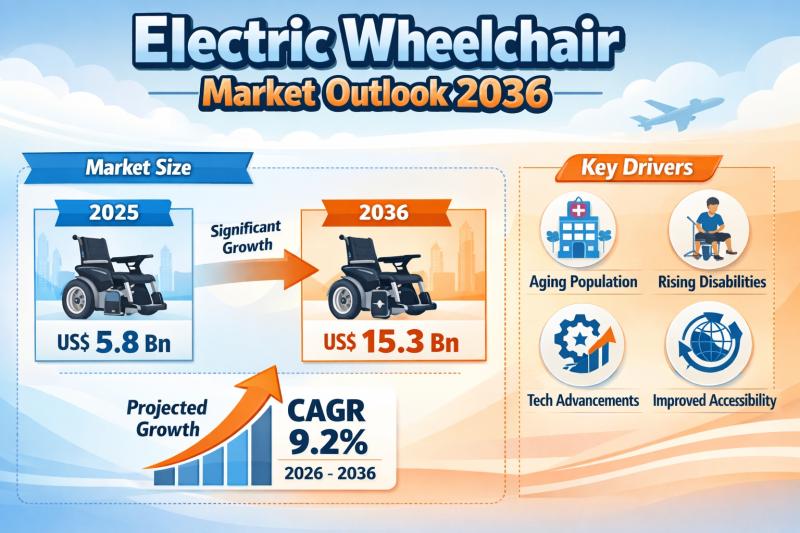
Electric Wheelchair Market Expanding at 9.2% CAGR Through 2036 - By Control Type …
The global electric wheelchair market continues to demonstrate strong and sustained growth, fueled by demographic transitions, technological innovation, and expanding healthcare access worldwide. Valued at US$ 5.8 billion in 2025, the market is projected to reach US$ 15.3 billion by 2036, expanding at a compound annual growth rate (CAGR) of 9.2% from 2026 to 2036.
Discover essential conclusions and data from our Report in this sample -
https://www.transparencymarketresearch.com/sample/sample.php?flag=S&rep_id=4198
This robust trajectory reflects rising…

Vehicle Predictive Maintenance Market Size Forecast to USD 13.7 Billion by 2036 …
Vehicle Predictive Maintenance Market Outlook 2036
The global vehicle predictive maintenance market was valued at USD 3 Billion in 2025 and is projected to reach USD 13.7 Billion by 2036, expanding at a robust CAGR of 14.7% from 2026 to 2036. Market growth is driven by increasing adoption of connected vehicles, rising fleet digitalization, advancements in AI-driven analytics, and growing emphasis on minimizing vehicle downtime and maintenance costs.
👉 Get your sample…
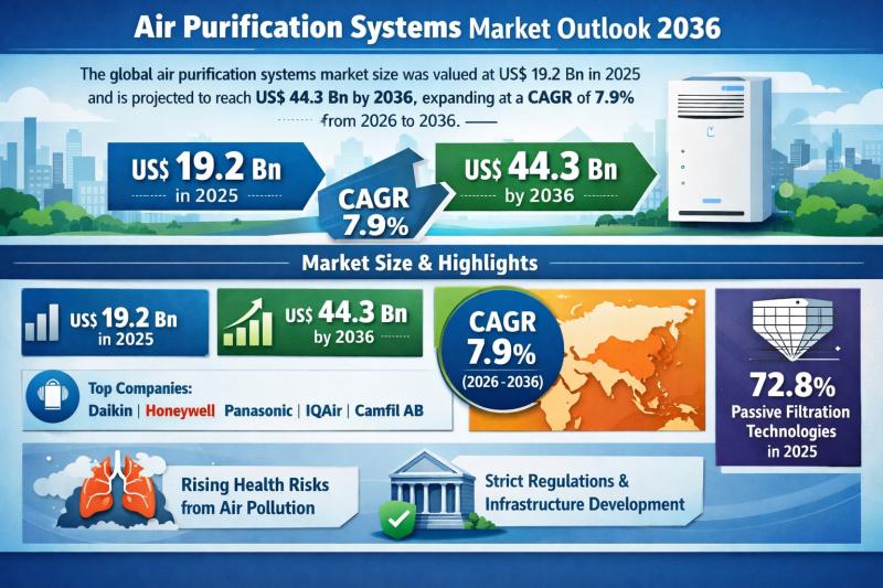
Global Air Purification Systems Market to Reach USD 44.3 Billion by 2036 at 7.9% …
The global Air Purification Systems Market was valued at US$ 19.2 Bn in 2025 and is projected to expand to US$ 44.3 Bn by 2036, registering a compound annual growth rate (CAGR) of 7.9% from 2026 to 2036. The market's upward trajectory reflects the structural shift in indoor air quality (IAQ) management, moving from discretionary consumer spending to mission-critical infrastructure investment.
With historical data available from 2021 to 2024, the industry…
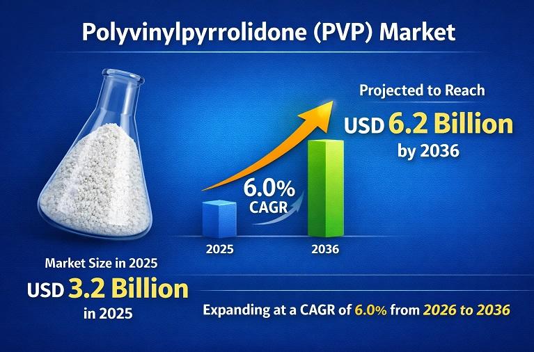
Polyvinylpyrrolidone (PVP) Market to Reach USD 6.2 Billion by 2036 Driven by Pha …
The Polyvinylpyrrolidone (PVP) Market was valued at around US$ 3.2 billion in 2025 and is projected to reach approximately US$ 6.2 billion by 2036, expanding at a steady CAGR of about 6.0% during the forecast period. This growth is primarily driven by rising demand from the pharmaceutical industry, where PVP is widely used as a tablet binder, solubilizer, and stabilizer, along with increasing consumption in cosmetics and personal care products…
More Releases for Wafer
Semiconductor Silicon Wafer Market Is Going to Boom |• Silicon Wafer • Globa …
Worldwide Market Reports has released a new in-depth research study on the "Semiconductor Silicon Wafer Market," highlighting strong growth potential in the coming years. The report delivers a structured and data-driven analysis of the market landscape, combining robust research methodology, market sizing, validated data modeling, and insights sourced from reliable primary and secondary channels.
The study thoroughly examines key market aspects, including growth drivers, restraints, challenges, emerging opportunities, technological advancements, innovation…
Semiconductor Wafer Electrostatic Chucks for 300mm Wafer Market Size, Trends & F …
Semiconductor Wafer Electrostatic Chucks for 300mm Wafer Market Size
The global Semiconductor Wafer Electrostatic Chucks for 300mm Wafer market is projected to grow from US$ 1227 million in 2024 to US$ 1672.7 million by 2030, at a Compound Annual Growth Rate (CAGR) of 5.3% during the forecast period.
Get Free Sample: https://reports.valuates.com/request/sample/QYRE-Auto-38F13137/Global_Semiconductor_Wafer_Electrostatic_Chucks_for_300mm_Wafer_Market_Research_Report_2023?utm_source=openpr&utm_medium=referral
The US & Canada market for Semiconductor Wafer Electrostatic Chucks for 300mm Wafer is estimated to increase from $ million in…
Wafer Hybrid Bonding Equipment Market Share Driven by Wafer-to-Wafer Technology …
Wafer Hybrid Bonding Equipment Market Size
The global market for Wafer Hybrid Bonding Equipment was valued at US$ 164 million in the year 2024 and is projected to reach a revised size of US$ 756 million by 2031, growing at a CAGR of 24.7% during the forecast period.
View sample report
https://reports.valuates.com/request/sample/QYRE-Auto-31W14822/Global_Wafer_Hybrid_Bonding_Equipment_Market_Insights_Forecast_to_2029
The Wafer Hybrid Bonding Equipment market is experiencing accelerated growth, driven by increasing demand for advanced semiconductor packaging technologies that enable higher…
Semiconductor Wafer Electrostatic Chucks for 300mm Wafer Market
Semiconductor Wafer Electrostatic Chucks for 300mm Wafer Market
The global Semiconductor Wafer Electrostatic Chucks for 300mm Wafer market was valued at US$ 1165 million in 2023 and is anticipated to reach US$ 1672.7 million by 2030, witnessing a CAGR of 5.3% during the forecast period 2024-2030.
View Sample Report
https://reports.valuates.com/request/sample/QYRE-Auto-38F13137/Global_Semiconductor_Wafer_Electrostatic_Chucks_for_300mm_Wafer_Market_Research_Report_2023
Report Scope
The Semiconductor Wafer Electrostatic Chucks for 300mm Wafer market size, estimations, and forecasts are provided in terms of output/shipments (Units) and revenue…
Automatic Mounter Wafer Equipment Market Report 2018: Segmentation by Type (100 …
Global Automatic Mounter Wafer Equipment market research report provides company profile for Lintec Corporation, Nitto Denko, Tokyo Electron, Technovision, Takatori, Ultron Systems, DISCO Corp., Syagrus Systems, Advanced Dicing Technologies, Longhill Industries and Others.
This market study includes data about consumer perspective, comprehensive analysis, statistics, market share, company performances (Stocks), historical analysis 2012 to 2017, market forecast 2018 to 2025 in terms of volume, revenue, YOY growth rate, and CAGR for…
EMEA Solar Wafer Cutting Fluid PEG Market For Semiconductor, Solar Wafer, Crysta …
Latest industry research report on: EMEA (Europe, Middle East and Africa) Solar Wafer Cutting Fluid PEG Market : Industry Size, Share, Research, Reviews, Analysis, Strategies, Demand, Growth, Segmentation, Parameters, Forecasts
Request For Sample Report @ https://www.marketresearchreports.biz/sample/sample/1194694
Geographically, this report split EMEA into Europe, the Middle East and Africa, With sales (K MT), revenue (Million USD), market share and growth rate of Solar Wafer Cutting Fluid PEG for these regions, from 2012 to…
