Press release
Driving Innovation in Semiconductor Packaging with Key Developments by Silicon Box and Onto Innovation
Get All the Details in Our Solution - Download Brochure : https://www.towardspackaging.com/download-brochure/5246
What is Panel Level Packaging?
Panel Level Packaging is a cutting-edge technique used in semiconductor packaging, where the package is processed on a square or rectangular surface, typically referred to as a panel. This process encompasses several key steps, including panel-level molding, bumping, die attach, and redistribution line (RDL) fabrication. These processes enable the creation of fine feature substrates, which are essential for the miniaturization and enhancement of electronic devices. Unlike traditional packaging methods that rely on individual package substrates, PLP focuses on the use of larger panel-sized substrates, offering significant advantages in both efficiency and cost-effectiveness.
Driving Forces Behind Market Growth
The growing demand for smaller, more powerful electronic devices is one of the key drivers of the PLP market. With the continuous development of products such as smartphones, wearables, Internet of Things (IoT) devices, and more, the need for packaging solutions that can support high-performance components in increasingly compact formats has become more critical. As the electronics industry pushes the boundaries of miniaturization, the need for innovative packaging techniques, like PLP, that can deliver reliable performance while maintaining cost efficiency is clear.
Another major factor fueling market growth is the advancement of technologies such as Artificial Intelligence (AI), 5G connectivity, and automotive technologies. These technologies require complex, high-performance components that benefit greatly from advanced packaging solutions like PLP. For example, in the realm of AI and 5G, the demand for heterogeneous integration, where different types of chips are combined into a single package, is driving innovation in packaging solutions. Panel Level Packaging is well-suited to this trend, as it can accommodate the intricate integration of multiple chip types into a compact form factor.
Automotive Sector Driving Innovation
The automotive sector is also a significant player in the growing demand for PLP. As the industry shifts toward advanced driver-assistance systems (ADAS) and electric vehicles (EVs), the need for high-performance electronic components, such as sensors and chips, is skyrocketing. These components require robust and compact packaging solutions that PLP can provide. PLP enables the integration of more advanced features while reducing the overall size and weight of components, making it an ideal solution for automotive applications.
The Future of Panel Level Packaging: What's Next?
Looking ahead, the panel level packaging market is set to witness continuous evolution, driven by ongoing advancements in manufacturing techniques and materials. The ability to leverage multiple infrastructures-such as Silicon (Si), Back-End-of-Line (BEOL) technologies, printed circuit boards (PCBs), LCD, and photovoltaics-is opening up new possibilities for producing high-quality packaging solutions. These innovative infrastructures are helping to improve the reliability and performance of electronic devices while keeping costs under control.
The market's expansion is also attributed to the growing trend of heterogeneous integration, where diverse chips are integrated into a single package, offering high levels of performance with reduced power consumption. This trend is particularly relevant in applications like smartphones, IoT devices, and automotive systems, where size, performance, and efficiency are of utmost importance.
Moreover, advancements in manufacturing are making it increasingly feasible to produce panel-level packages at scale. This opens up new opportunities for industries seeking to implement next-gen packaging at competitive prices.
Key Trends and Insights Shaping the Panel-Level Packaging Market
As the demand for more compact, high-performance electronic devices continues to grow, Panel-Level Packaging (PLP) has emerged as a transformative solution in the semiconductor industry. This innovative packaging technique, which shifts traditional semiconductor packing to a larger-panel configuration, is set to play a pivotal role in meeting the ever-increasing need for miniaturized, highly efficient devices. Let's take a closer look at the key trends and findings shaping the future of the PLP market.
Driving Cost Efficiency with Economies of Scale
Panel-level packaging is revolutionizing the semiconductor industry by enabling significant cost savings through economies of scale and enhanced production efficiency. By utilizing larger panels, manufacturers can increase throughput and reduce per-unit costs, making PLP an attractive option for industries striving to meet the growing demand for smaller yet more powerful electronic components. This shift towards panel-based configurations offers a scalable approach to semiconductor packaging, providing manufacturers with a more efficient means of producing high-performance components.
A crucial milestone in the adoption of PLP came with the introduction of SEMI Standard 3D20 in 2019, which standardized panel sizes across the industry. This standardization opened the door for equipment manufacturers to invest in specialized tools and equipment designed to facilitate the PLP process. As a result, companies have been able to optimize their production lines and improve the overall cost-effectiveness of PLP technology.
The Rise of Glass Substrates in Semiconductor Packaging
In recent years, glass substrates have gained significant attention within the semiconductor industry. Known for their excellent electrical properties, glass substrates are increasingly being used in high-frequency applications, such as 5G and IoT devices. The shift towards glass is driven by its superior performance in high-frequency environments, offering a promising alternative to traditional materials like silicon and ceramics.
Companies with extensive experience in the production of glass wafers and panels are poised to make a significant impact as this trend gains momentum. These companies are at the forefront of a technological shift that could redefine the way semiconductor components are packaged, offering manufacturers a new avenue for creating highly efficient, compact devices.
The Technological Push for Smaller, Smarter Devices
The demand for smaller electronic devices with greater capabilities, memory, and speed is being propelled by several key technological advancements, including 5G, Internet of Things (IoT), virtual and augmented reality, and autonomous driving. These industries require semiconductor components that can meet the ever-increasing need for high-performance, energy-efficient devices. As a result, semiconductor packaging solutions, including PLP, are becoming more crucial than ever in enabling these technologies to reach their full potential.
Manufacturers are under immense pressure to develop packaging solutions that support the miniaturization of these devices while maintaining or even enhancing their performance. As semiconductors are the cornerstone of modern electronics, their ability to meet these demands is essential for driving the progress of new technologies.
Advanced IC Packaging Methods and Thermal Management
Advanced integrated circuit (IC) packaging techniques are paving the way for the most recent panel-level packing methods. These methods are not only improving the efficiency of packaging but also ensuring that critical components are shielded from the harsh effects of high-temperature manufacturing processes. As the demand for faster, smaller devices grows, managing heat becomes a more significant challenge.
Thermal control has become a critical concern as the electronics industry moves toward greater integration and miniaturization. As components get smaller and more powerful, the need to manage heat more effectively has never been greater. Effective thermal resistance management relies on several key factors, including heat transfer paths, conductivity, and transfer surface area. As the industry moves toward smaller components, reducing thermal resistance becomes more challenging. However, advancements in materials and packaging techniques are helping to mitigate these challenges, ensuring that devices can perform optimally without overheating.
Regional Growth: Asia-Pacific and North America Lead the Way
The Asia-Pacific region is set to experience the fastest growth in the panel-level packaging market, with a projected CAGR of 40.89% during the forecast period. This rapid growth is driven by the booming demand for consumer electronics and IoT applications, as well as significant investments in semiconductor manufacturing. As countries like China, South Korea, and Taiwan continue to expand their semiconductor production capabilities, the Asia-Pacific region is becoming the epicenter of PLP innovation and adoption.
On the other hand, North America held a considerable share of 30.82% of the market in 2023. This dominance can be attributed to the region's advanced technological developments and the high demand for cutting-edge electronics. Moreover, North America is seeing increasing investments in research and development (R&D), particularly in sectors like automotive, aerospace, and consumer electronics. The region's focus on innovation, coupled with its strong manufacturing base, positions it well to capitalize on the growing demand for advanced semiconductor packaging solutions like PLP.
Browse More Insights:
Wafer Level Packaging Market: https://www.towardspackaging.com/insights/wafer-level-packaging-market-sizing
Panel Level Packaging Market: https://www.towardspackaging.com/insights/panel-level-packaging-market-sizing
Polyethylene Films Market: https://www.towardspackaging.com/insights/polyethylene-films-market-sizing
Pharmaceutical Glass Packaging Market: https://www.towardspackaging.com/insights/pharmaceutical-glass-packaging-market-sizing
Coffee Bags Market: https://www.towardspackaging.com/insights/coffee-bags-market-sizing
Packaging Printing Market:https://www.towardspackaging.com/insights/packaging-printing-market-sizing
Child Resistant Packaging Market: https://www.towardspackaging.com/insights/child-resistant-packaging-market-sizing
Carton Packaging Market: https://www.towardspackaging.com/insights/carton-packaging-market-sizing
Electronic Packaging Market: https://www.towardspackaging.com/insights/electronic-packaging-market-sizing
Virgin Plastic Packaging Market: https://www.towardspackaging.com/insights/virgin-plastic-packaging-market-sizing
Recent Developments by Key Market Players in the Panel-Level Packaging Market
The panel-level packaging (PLP) market is witnessing a surge of activity from key players, each pushing the boundaries of semiconductor assembly and packaging to meet the evolving demands of next-generation technologies. Recent announcements highlight significant investments and innovations by leading companies, signaling an exciting future for PLP. Let's explore some of the most notable developments.
Silicon Box's Bold Expansion Plans
In a move that underscores the growing importance of panel-level packaging in semiconductor manufacturing, Silicon Box, a state-of-the-art PLP foundry, has revealed its ambitious plan to collaborate with the Italian government on a major expansion. The company intends to invest up to $3.6 billion (€3.2 billion) to develop a new, cutting-edge semiconductor assembly and testing facility in Northern Italy. This facility, set to be completed by 2028, will significantly boost the production capacity needed to meet the increasing demand for advanced packaging solutions.
The new facility will be modeled after Silicon Box's flagship foundry in Singapore, which is renowned for its industry-leading semiconductor packaging capabilities. Over the course of several years, Silicon Box plans to replicate the success of its Singapore operations, ensuring that the Italian facility incorporates the latest packaging technologies, including 3D integration and testing capabilities. This expansion is expected to play a pivotal role in addressing the growing demand for next-generation semiconductor devices, providing manufacturers with the necessary packaging solutions to keep pace with technological advancements.
This strategic move by Silicon Box is a clear indication of the company's
commitment to staying ahead in the highly competitive PLP market. By investing in advanced packaging capabilities and testing infrastructure, Silicon Box is positioning itself as a key player in meeting the evolving needs of industries such as 5G, IoT, and autonomous driving, all of which require smaller, more efficient semiconductor components.
Onto Innovation Inc. and the Establishment of a New Applications Center of Excellence
In another exciting development within the panel-level packaging sector, Onto Innovation Inc. has taken significant strides to enhance its role in the burgeoning chiplet market. The company has recently announced the establishment of an Applications Center of Excellence, a facility dedicated to advancing panel-level packaging technologies. This facility will focus on a range of critical activities, including tool demonstration, photoresist qualification, process integration, and research and development (R&D) efforts aimed at optimizing PLP processes.
Onto Innovation's investment in this facility comes at a time when the chiplet package market is set for rapid growth. According to TechSearch International, the market for chiplet packaging is projected to expand at an average annual rate of 103% over the next three years. This explosive growth highlights the growing importance of packaging technologies like PLP, which enable the integration of multiple smaller semiconductor components (chiplets) into a single, highly functional package.
The new Applications Center of Excellence will serve as a critical hub for innovation and collaboration, providing Onto Innovation with the tools and resources necessary to develop the next generation of PLP solutions. As the company continues to push the envelope in semiconductor packaging, this new facility will play a central role in ensuring Onto Innovation remains at the forefront of the chiplet revolution.
The Road Ahead: Panel-Level Packaging's Growing Role in Semiconductor Manufacturing
These recent developments from Silicon Box and Onto Innovation reflect a broader trend in the semiconductor industry, where companies are increasingly turning to panel-level packaging to address the challenges posed by miniaturization, integration, and the need for higher performance. As industries like 5G, AI, and autonomous vehicles demand more powerful, smaller semiconductor components, the ability to scale production and integrate multiple chiplets into a single package will become a crucial factor in the success of these technologies.
With Asia-Pacific leading the charge in PLP adoption and North America focusing on R&D and innovation, the global panel-level packaging market is poised for significant growth in the coming years. The strategic investments made by key players like Silicon Box and Onto Innovation will undoubtedly accelerate this growth, ensuring that the semiconductor industry is ready to meet the demands of tomorrow's technologies.
As panel-level packaging continues to evolve, it is clear that the industry is entering an exciting new phase of innovation. With the combined efforts of established players and new entrants alike, the future of semiconductor packaging looks bright, offering the potential for faster, more efficient, and highly integrated electronic devices.
Baner
Invest in Our Premium Strategic Solution: https://www.towardspackaging.com/price/5246
Review the Full TOC for the Panel Level Packaging Market Report: https://www.towardspackaging.com/table-of-content/panel-level-packaging-market-sizing
Get the latest insights on industry segmentation with our Annual Membership https://www.towardshealthcare.com/get-an-annual-membership
About Us
Towards Healthcare is a leading global provider of technological solutions, clinical research services, and advanced analytics to the healthcare sector, committed to forming creative connections that result in actionable insights and creative innovations. We are a global strategy consulting firm that assists business leaders in gaining a competitive edge and accelerating growth. We are a provider of technological solutions, clinical research services, and advanced analytics to the healthcare sector, committed to forming creative connections that result in actionable insights and creative innovations.
We've prepared a service to support you. Please feel free to contact us at sales@towardshealthcare.com
Web: https://www.towardshealthcare.com
For Latest Update Follow Us: https://www.linkedin.com/company/towards-healthcare
This release was published on openPR.
Permanent link to this press release:
Copy
Please set a link in the press area of your homepage to this press release on openPR. openPR disclaims liability for any content contained in this release.
You can edit or delete your press release Driving Innovation in Semiconductor Packaging with Key Developments by Silicon Box and Onto Innovation here
News-ID: 3826666 • Views: …
More Releases from Towards Packaging
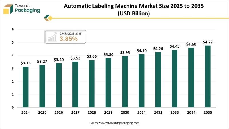
Automatic Labeling Machine Market Set for Strong Growth Through 2035
The global automatic labeling machine market is poised for steady expansion, rising from USD 3.4 billion in 2026 to USD 4.77 billion by 2035 at a CAGR of 3.85%. Demand is being driven by rapid automation in packaging lines, stringent labeling regulations, and the shift toward high-speed, error-free production across industries.
Download Sample: https://www.towardspackaging.com/download-sample/5882
Self-adhesive labeling systems currently hold the largest share at 39%, supported by their versatility and cost efficiency. Meanwhile,…

Unleashing Growth in the Liquid Packaging Market with Strategic Innovations
The liquid packaging industry is experiencing remarkable growth, with projections indicating an increase from USD 397.36 billion in 2025 to USD 645.43 billion by 2034. This growth, at a compound annual growth rate (CAGR) of 5.7%, signifies the expanding demand for liquid packaging solutions across a variety of sectors. As we delve into the market dynamics, it becomes clear that the liquid packaging sector is evolving rapidly, with several key…

Advancements in Hot-Fill Food Packaging Paving the Way for a Sustainable Future
The global hot-fill food packaging market is experiencing a steady rise, with an expected market value of USD 71.26 billion by 2033, up from USD 49.85 billion in 2023. This growth is projected to follow a compound annual growth rate (CAGR) of 3.76% from 2024 to 2033, reflecting the increasing demand for innovative packaging solutions in the food and beverage sector.
Download a Brochure of Hot-fill Food Packaging Market: https://www.towardspackaging.com/download-brochure/5266
Hot-Fill…

Driving Growth and Innovation in the Plastic Bag Market
The plastic bag market is undergoing significant growth, with its value reaching an estimated US$ 25.10 billion in 2023. Projections suggest that this market could hit a substantial US$ 35.41 billion by 2033, marking a steady compound annual growth rate (CAGR) of 3.5% from 2024 to 2034. This growth is largely driven by the expanding needs of various industries for efficient and cost-effective packaging solutions.
Download a Brochure of Plastic Bag…
More Releases for PLP
Helical Vibration Dampers Market Innovations and Key Players: Huaneng Electric P …
The Helical Vibration Dampers market has emerged as a pivotal segment in the landscape of industrial applications, offering essential solutions for managing and mitigating vibrations in various settings. These specialized devices play a critical role in enhancing the stability and longevity of structures, equipment, and transmission systems, making them indispensable in sectors such as energy, telecommunications, and transportation.
𝐘𝐨𝐮 𝐜𝐚𝐧 𝐚𝐜𝐜𝐞𝐬𝐬 𝐚 𝐬𝐚𝐦𝐩𝐥𝐞 𝐏𝐃𝐅 𝐫𝐞𝐩𝐨𝐫𝐭 𝐡𝐞𝐫𝐞: https://www.statsndata.org/download-sample.php?id=349830
In recent years, the Helical…
Patient Lift Pendant (PLP) Market Giants' Expenditure Will Increase with a CAGR …
The "Global Patient Lift Pendant (PLP)" intelligence report, just published by USD Analytics, covers insurers' micro-level study of important market niches, product offers, and sales channels. In order to determine market size, potential, growth trends, and competitive environment, the Global Patient Lift Pendant (PLP) provides dynamic views. Both primary and secondary sources of data were used to generate the research, which has both qualitative and quantitative depth. Several of the…
Bird Flapper Market Manufacturers, Suppliers, Vendors Sales, Revenue, Market Sha …
"Strategic Market Insights for Every Sector: Explore Our Comprehensive Bird Flapper Industry Research Report 2023-2029. Inform Your Business Decisions Today!"
The latest report provides information about the global Bird Flapper market and forecasts the growth prospects and industry trends that could emerge between 2023 and 2029. Future growth was calculated by taking the current growth rate and the entire market size into account. The Bird Flapper Market report offers in-depth qualitative…
Performed Lashing Rods Market to Show Incredible Growth and Forecast by 2029 | P …
Global Performed Lashing Rods Market Overview
The Performed Lashing Rods market is a diverse and rapidly evolving industry that encompasses a wide range of products and services. It is characterized by intense competition, changing consumer preferences, and technological advancements that continually drive innovation.
The Performed Lashing Rods market is comprised of several sub-sectors, including but not limited to: electronics, healthcare, automotive, consumer goods, and energy. Each of these sub-sectors has its unique…
Global Interphase Spacer System Market Analysis, Competitors, Growth Rate 2023 | …
Global Info Research announces the release of the report "Global Interphase Spacer System Market 2023 by Manufacturers, Regions, Type and Application, Forecast to 2029" . The report is a detailed and comprehensive analysis presented by region and country, type and application. As the market is constantly changing, the report explores the competition, supply and demand trends, as well as key factors that contribute to its changing demands across many markets. Company profiles and product examples of selected…
Patient Lift Pendant (PLP) Market Booming Worldwide( Forecast Period 2023-2029) …
The global Patient Lift Pendant (PLP) market is carefully researched in the report while largely concentrating on top players and their business tactics, geographical expansion, market segments, competitive landscape, manufacturing, and pricing and cost structures. Each section of the research study is specially prepared to explore key aspects of the global Patient Lift Pendant (PLP) market. For instance, the market dynamics section digs deep into the drivers, restraints, trends, and…
