Press release
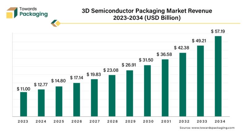
3D Semiconductor Packaging Market Size to Grow $57.19 Bn by 2034
Download Statistical Data: https://www.towardspackaging.com/download-statistics/5275
Driving Forces Behind the Market Growth
The primary force driving the expansion of the 3D semiconductor packaging market is the increasing demand for miniaturized electronic devices. As industries push for smaller, more powerful devices that offer enhanced performance, the need for 3D packaging technologies has surged. 3D semiconductor packaging provides an effective solution to meet the miniaturization requirements while maintaining the high performance expected from modern electronics.
Miniaturization is essential for various industries, including consumer electronics, automotive, telecommunications, and healthcare, all of which are demanding more compact yet powerful devices. This trend is particularly noticeable in mobile phones, wearable technologies, automotive systems, and IoT (Internet of Things) devices. The ability of 3D packaging to pack more functionality into smaller, more efficient packages makes it indispensable for future product development.
The Role of Advanced Technology
Another critical factor influencing the growth of the 3D semiconductor packaging market is the adoption of advanced manufacturing technologies. As semiconductor companies increasingly turn to 3D packaging to address the challenges of space limitations and performance optimization, there has been a significant rise in the development of cutting-edge manufacturing processes. These advanced technologies allow for more complex and high-performing packaging solutions, catering to industries that require high-density interconnects and enhanced thermal management.
To stay competitive, key players in the semiconductor packaging industry are investing in research and development (R&D) to create innovative packaging solutions. The rise of technologies such as Through-Silicon Via (TSV), system-in-package (SiP), and fan-out wafer-level packaging (FOWLP) are pivotal in transforming the industry. These innovations enable the production of smaller, faster, and more efficient chips, further fueling the growth of the 3D semiconductor packaging market.
Mergers and Acquisitions: Shaping the Future
The 3D semiconductor packaging market is witnessing an uptick in mergers and acquisitions (M&A) as key players seek to bolster their technological capabilities and expand their market reach. Companies are increasingly adopting inorganic growth strategies, acquiring smaller firms with specialized expertise in semiconductor packaging technologies. This approach allows larger companies to accelerate the development of advanced packaging solutions and strengthen their position in the highly competitive market.
The acquisition of cutting-edge intellectual property (IP) and the integration of advanced manufacturing technologies from these smaller firms are essential in keeping pace with the fast-evolving demands of the electronics industry. These strategic moves also enable companies to offer a more comprehensive range of packaging solutions, positioning them to better serve the needs of a diverse customer base.
Regional Insights: A Global Perspective
The 3D semiconductor packaging market is experiencing growth across various regions, with key players leveraging global trends to expand their presence in emerging and developed markets alike. North America, Asia-Pacific, and Europe are the primary regions driving the market's expansion.
• North America: The United States remains a dominant force in the semiconductor industry, with leading companies in the 3D semiconductor packaging market, including Intel and Qualcomm, paving the way for technological advancements. The region is witnessing increased investment in R&D and manufacturing infrastructure to support the growing demand for 3D packaging technologies.
• Asia-Pacific: The Asia-Pacific region is expected to experience the fastest growth in the 3D semiconductor packaging market. China, Japan, and South Korea are home to some of the largest semiconductor manufacturers globally. As these nations continue to push for innovation in electronics, the demand for 3D semiconductor packaging is set to increase significantly.
• Europe: Europe is also playing a significant role in the development of 3D semiconductor packaging technologies, with countries like Germany and the Netherlands investing heavily in semiconductor research and development. The region's focus on high-performance computing and automotive applications is driving the adoption of advanced packaging solutions.
The Growing Impact of 3D Semiconductor Packaging: Key Insights and Market Trends
As technology continues to evolve, so does the way we design and manufacture the electronic devices that power our modern world. One of the most significant advancements in the semiconductor industry is the rise of 3D semiconductor packaging, a technology that is transforming the way electronic devices are developed. This article delves into the key insights, benefits, and driving forces behind the growth of the 3D semiconductor packaging market, providing an in-depth look at this cutting-edge innovation.
Key Insights of the 3D Semiconductor Packaging Market
Asia Pacific has dominated the 3D semiconductor packaging market in 2024, driven by the region's strong manufacturing capabilities and the presence of leading semiconductor companies. With rapid advancements in electronics and technology, Asia Pacific remains at the forefront of innovation in semiconductor packaging.
However, North America is expected to experience significant growth throughout the forecast period. This growth is attributed to the region's growing demand for high-performance computing, data centers, and cutting-edge consumer electronics. As technology giants continue to push the boundaries of semiconductor design, North America is poised to benefit from this expansion.
In terms of technology, the 3D Through Silicon Via (TSV) segment held the largest share in 2024. TSV technology is a crucial aspect of 3D semiconductor packaging, enabling the vertical stacking of chips and facilitating higher performance and compactness. This technology is being widely adopted due to its ability to reduce signal travel time, improve bandwidth, and reduce latency in high-speed applications.
Regarding material, the organic substrate segment is expected to see significant growth during the forecast period. Organic substrates are crucial for providing the foundation on which the semiconductor devices are built. Their flexibility, cost-effectiveness, and ease of manufacture are making them an attractive option for 3D semiconductor packaging applications.
Automotive and transport emerged as the dominant industrial vertical for 3D
semiconductor packaging in 2024. With the rise of autonomous vehicles, advanced driver-assistance systems (ADAS), and electric vehicles (EVs), the demand for smaller, more efficient semiconductor devices in automotive applications has surged. As automotive technology continues to advance, 3D semiconductor packaging will play a pivotal role in meeting the industry's performance and miniaturization requirements.
Miniaturization of Electronic Devices: The Role of 3D Semiconductor Packaging
3D semiconductor packaging refers to the innovative integration of multiple semiconductor devices into a single package, stacked in a three-dimensional configuration. Unlike traditional 2D packaging, where components are laid out flat, 3D packaging enables chips to be stacked vertically, offering a compact and efficient solution for modern electronic devices. This technology is particularly useful in mobile and wearable electronics, where space constraints are a significant challenge.
There are various types of technologies used in 3D packaging, each with its unique advantages:
• Through Silicon Via (TSV) Technology: TSV technology allows for the vertical stacking of chips, creating shorter interconnects and enabling high-performance applications with lower latency and higher bandwidth.
• Wafer-Level Packaging (WLP): WLP is a cost-effective solution for 3D packaging, offering benefits such as reduced footprint and improved reliability for high-density devices.
• System-in-Package (SiP): SiP integrates multiple components (such as processors, memory, and sensors) into a single package, enabling enhanced functionality in a compact form factor.
• Chip-on-Wafer (CoW) and Wafer-on-Wafer (WoW): These techniques allow for the bonding of chips directly to a wafer, enabling further miniaturization and better thermal management.
Benefits of 3D Semiconductor Packaging
The adoption of 3D semiconductor packaging brings several key benefits to the table, which are driving its rapid growth and adoption in the electronics industry:
1. Space Efficiency: By stacking multiple chips vertically, 3D packaging reduces the overall size of electronic devices, making them more compact and suitable for applications in mobile phones, wearables, and other space-constrained devices.
2. Performance Improvements: The shorter interconnects in 3D packaging lead to lower latency and higher data transfer speeds. This is crucial for applications in high-performance computing, data centers, and memory-intensive devices, where speed is of the essence.
3. Thermal Management: While traditional packaging methods can face challenges with heat dissipation, 3D packaging can improve thermal management by optimizing the arrangement of components and using advanced materials to enhance heat dissipation.
4. Power Efficiency: Shortening the distance that signals travel within a chip can reduce power consumption, which is vital for battery-powered devices like smartphones and wearables. This makes 3D semiconductor packaging an attractive solution for energy-conscious consumers and manufacturers.
5. Design Flexibility: 3D packaging offers greater flexibility in device design, allowing manufacturers to integrate a wider range of functionalities into a single device, without compromising on size or performance.
The Future of 3D Semiconductor Packaging
3D semiconductor packaging technology is positioned to play a crucial role in the future of electronics and semiconductor manufacturing. As the demand for smaller, more powerful, and energy-efficient devices continues to rise, 3D packaging offers a viable solution to meet these needs. However, the technology is not without its challenges. Manufacturing complexities, heat dissipation, and reliability concerns need to be addressed as the industry moves forward.
Despite these challenges, 3D semiconductor packaging is driving significant advancements in the miniaturization and performance of electronic devices. As companies continue to innovate, the technology is expected to play a key role in the development of next-generation consumer electronics, automotive systems, and data centers.
Key Factors Driving Market Growth
Several factors are contributing to the accelerated growth of the 3D
semiconductor packaging market:
1. Geographic Expansion: Electronic companies are increasingly focused on expanding their operations into new regions, particularly in emerging markets. This geographic expansion is expected to fuel the growth of the 3D semiconductor packaging market in the coming years.
2. Cost Reduction and Production Efficiency: As manufacturers seek to reduce costs and improve production efficiency, 3D semiconductor packaging offers an attractive option. The integration of multiple devices into a single package reduces the need for separate components, cutting down on production costs.
3. Emerging Markets: The demand for advanced 3D semiconductor packaging is increasing in emerging markets, where electronics manufacturing is expanding rapidly. This trend is expected to drive global market growth.
4. Regulatory Support: Governments and regulatory bodies are providing increasing support for the development and adoption of advanced semiconductor technologies, further driving the growth of the 3D semiconductor packaging market.
5. Performance Enhancement: As the need for higher performance and reduced latency grows, 3D semiconductor packaging becomes an essential technology for high-performance computing, data centers, and other data-intensive applications. The push for enhanced performance continues to be a major driver of market growth.
AI in the 3D Packaging Industry: Revolutionizing Semiconductor Solutions
The integration of Artificial Intelligence (AI) into the 3D packaging industry is bringing transformative changes, particularly in the semiconductor sector. AI's application in 3D semiconductor packaging provides significant advancements across various stages of design, manufacturing, and performance optimization. As the demand for compact, high-performance electronic devices continues to grow, AI is poised to play a pivotal role in shaping the future of this industry.
AI Enhancing 3D Packaging Design and Performance
AI can streamline the design process by optimizing layouts and improving component integration. Through advanced algorithms, AI is able to analyze large datasets, enabling designers to achieve optimal space utilization within a 3D package. This can dramatically reduce signal interference and improve the overall efficiency of the design. Additionally, AI tools can simulate and predict thermal and electrical behavior, providing valuable insights during the design phase. This allows designers to identify potential performance issues before physical prototypes are created, saving time and resources.
Moreover, AI has the ability to enhance testing and validation processes. By using machine learning models, AI can predict and detect potential defects in 3D packaging systems with higher precision, ensuring consistent quality. This leads to improved product reliability and faster time-to-market for new semiconductor components. The combination of optimized design and enhanced testing techniques results in a more efficient, cost-effective approach to semiconductor packaging, driving innovation and competitiveness in the industry.
Impact of AI-Driven Automation on Manufacturing
AI-driven automation is another key area where the technology is transforming the 3D packaging sector. In semiconductor manufacturing, where precision and speed are critical, AI can streamline processes to reduce cycle times and minimize human error. Machine learning algorithms can monitor production lines in real-time, identifying defects early in the process and making adjustments autonomously to maintain quality standards. This results in higher throughput, reduced production costs, and improved consistency, making it a game-changer for manufacturers in the highly competitive semiconductor market.
The Role of the Automotive Industry in Driving 3D Packaging Demand
One of the key drivers fueling the growth of the 3D semiconductor packaging market is the expansion of the automotive industry, particularly with the rise of electric vehicles (EVs) and advanced driver-assistance systems (ADAS). These vehicles require high-performance electronics to manage complex functions such as power conversion, energy storage, and sensor integration. 3D packaging is an ideal solution, offering space optimization and enhanced thermal management, both of which are critical in the compact environments of EVs.
As EVs gain traction in the market, driven by the desire for more sustainable alternatives to traditional gasoline-powered vehicles, the demand for 3D packaging solutions is expected to grow significantly. 3D packaging reduces the physical footprint of semiconductor components, allowing for efficient use of space within the vehicle while maintaining high performance. As a result, EV manufacturers are increasingly turning to 3D packaging as a way to improve the functionality and efficiency of their vehicles.
Challenges: Regulatory Standards and Manufacturing Complexities
Despite the clear benefits, the 3D semiconductor packaging market faces certain challenges, particularly in meeting regulatory standards. The absence of industry-wide standards for 3D packaging complicates the manufacturing process, creating uncertainty in the supply chain. Manufacturers must navigate a complex web of regional regulations, which can slow the adoption of 3D packaging technologies and increase costs.
Moreover, the materials used in 3D packaging must be compatible to ensure reliability, but achieving this compatibility can be a challenge. Thermal expansion and mechanical strain are significant concerns when stacking chips in a 3D configuration. Additionally, the cost of advanced manufacturing processes, such as through-silicon vias (TSVs) and wafer-level packaging, can be prohibitive, especially for smaller companies with limited resources. Overcoming these technical and financial barriers will require continued innovation and investment in research and development.
Opportunities: Customization and Service Launches
The demand for smaller, more powerful electronic devices-such as smartphones, wearables, and IoT devices-has created a growing need for compact, high-performance packaging solutions. This trend is driving further adoption of 3D packaging technology. Key players in the market, including Intel, Samsung, and TSMC, are investing heavily in the development of 3D packaging services. These services aim to provide custom solutions that meet the specific needs of different industries, opening up lucrative opportunities for growth in the semiconductor packaging market.
One of the exciting opportunities in 3D packaging lies in its ability to offer highly customizable and personalized packaging solutions. As consumer demand for personalized products increases, manufacturers are looking for ways to create tailored packaging solutions for niche markets. 3D packaging's flexibility allows for such customization, enabling manufacturers to meet the unique needs of their clients. This versatility is expected to drive further demand in the coming years, as more businesses seek innovative packaging solutions that stand out in the marketplace.
Intel's Innovations in 3D Packaging and AI
Intel Corporation has made notable strides in advancing AI-driven 3D packaging technology. In February 2024, the company introduced an enhanced process roadmap aimed at bolstering its position as one of the world's leading foundries by 2030. Among the key advancements was the introduction of Intel 3-T, optimized with through-silicon vias (TSVs) for 3D advanced packaging designs. This innovation is set to improve performance, reduce power consumption, and enhance thermal management in 3D semiconductor packaging.
Intel's work with its partners is expected to lead to further breakthroughs in packaging technology, allowing for the integration of multiple semiconductors into a single package. This development has the potential to significantly impact industries ranging from consumer electronics to high-performance computing, where space and power efficiency are paramount.
The Dominance of 3D Through-Silicon Via (TSV) Technology
The TSV segment is expected to continue dominating the 3D semiconductor packaging market, with its widespread use in applications requiring high density, compact designs, and improved performance. TSVs allow for vertical stacking of chips, significantly reducing the overall footprint while enhancing functionality. The technology offers several advantages, including lower resistance, faster signal transmission, and improved thermal management. These benefits make TSVs particularly suitable for high-performance applications such as mobile devices, wearables, and high-performance computing.
In November 2023, United Microelectronics Corp (UMC) introduced its wafer-to-wafer (W2W) 3D IC project in collaboration with several industry leaders. This initiative aims to advance the production of 3D products, further driving the adoption of TSV technology in the semiconductor industry.
The Rapid Growth and Evolution of 3D Semiconductor Packaging: Key Segments and Regional Insights
The 3D semiconductor packaging market is poised for significant expansion between 2024 and 2034, driven by technological advancements, growing demand for compact electronics, and the proliferation of IoT, 5G, and autonomous systems. Among the various packaging techniques, 3D wire bonding is emerging as one of the fastest-growing segments, while organic substrates and automotive applications continue to play pivotal roles in shaping the market's trajectory. Additionally, the Asia-Pacific region remains at the forefront of this growth, supported by robust manufacturing ecosystems and technological innovation.
3D Wire Bonded Technology: Paving the Way for Space-Efficient, High-Performance Electronics
The 3D wire bonded segment is expected to grow at the fastest rate within the 3D semiconductor packaging market during the forecast period. 3D wire bonding, a cutting-edge packaging technique, enhances the performance, scalability, and functionality of integrated circuits, making it indispensable in the evolving electronics landscape.
One of the key advantages of 3D wire bonding is its ability to reduce the overall footprint of a device. By stacking multiple chips and using shorter interconnect lengths, this technology decreases resistance and boosts signal integrity, resulting in improved overall device performance. As a result, 3D wire bonding is particularly well-suited for compact devices such as smartphones, wearables, and IoT devices, where space is a premium.
In addition to space efficiency, 3D wire bonding offers cost-effective solutions. By reducing the package size and improving manufacturing efficiency, this technology lowers material and assembly costs. This is especially beneficial in high-volume production, as it allows for multi-chip integration that supports the incorporation of more complex functionalities into smaller devices. These features, combined with the scalability offered by 3D wire bonding, position this technology as a key enabler of the next generation of electronic devices.
Organic Substrates: Flexible, Cost-Effective, and Reliable
Organic substrates have carved a significant share in the 3D semiconductor packaging market, and this trend is expected to continue. In 2023, organic substrates held a notable portion of the market, primarily due to their flexibility, lightweight nature, and cost-effectiveness. These substrates, made from materials like epoxy resin and reinforced glass, are more adaptable and affordable compared to traditional ceramic or metal substrates, making them particularly attractive for high-volume semiconductor production.
The flexibility of organic substrates allows for the integration of complex designs and geometries, accommodating a wide range of chip sizes and configurations necessary for 3D packaging. They are well-suited for advanced consumer electronics, where yield rates, reliability, and sustainability are paramount. Organic substrates have demonstrated excellent performance in terms of reliability over time, and many variants are also more environmentally friendly, aligning with the industry's growing focus on sustainable practices.
Their lower cost, coupled with superior processing methods, makes organic substrates an ideal choice for applications where both cost and performance are critical factors. These attributes continue to propel their adoption in 3D semiconductor packaging, where performance and efficiency are crucial.
Automotive and Transportation: The Dominant Segment
The automotive and transportation segment is one of the leading drivers of growth in the 3D semiconductor packaging market. Modern vehicles increasingly rely on semiconductors to enable advanced driver-assistance systems (ADAS), such as adaptive cruise control, lane-keeping assist, and collision avoidance. As vehicles become smarter and more automated, the need for sophisticated semiconductor components continues to rise.
Electric vehicles (EVs), in particular, are driving demand for advanced semiconductor solutions in areas like battery management systems, power electronics, and electric drive controls. These components are vital for optimizing efficiency, improving performance, and reducing emissions in EVs. Furthermore, with the proliferation of autonomous vehicles, semiconductors play a crucial role in enabling technologies such as sensors, cameras, and LiDAR systems.
As the automotive industry pushes for greater fuel efficiency, safety, and performance, high-quality semiconductors become more critical for meeting stringent regulatory standards and consumer expectations. The trend towards electrification, automation, and connectivity is poised to continue driving demand for 3D semiconductor packaging solutions in the automotive sector.
Electronics: The Fastest Growing Segment
In terms of growth, the electronics segment is projected to expand at the fastest rate in the 3D semiconductor packaging market. The electronics industry has seen an increasing demand for smaller, more powerful devices, a trend that 3D packaging directly supports. 3D packaging enables the integration of multiple components into a compact package, reducing signal loss and latency while improving power efficiency and overall performance.
The benefits of 3D packaging in electronics are vast. By stacking chips and integrating multiple functionalities (e.g., logic, memory) into a single package, 3D packaging simplifies design and enhances device capabilities. It also allows for the integration of heterogeneous materials and technologies, such as combining analog, digital, and RF components, which is crucial in next-generation electronics. As consumer electronics devices, including smartphones, wearables, and IoT devices, continue to demand more processing power in smaller packages, 3D packaging will play a central role in enabling these innovations.
Asia-Pacific: Leading the Charge in Semiconductor Innovation
The Asia-Pacific region dominated the global 3D semiconductor packaging market in 2023, and it shows no signs of slowing down. The region is home to some of the world's largest semiconductor manufacturers, including major players in Taiwan, South Korea, and Japan, who have well-established semiconductor manufacturing ecosystems. These countries benefit from efficient manufacturing processes, competitive labor costs, and robust supply chains, positioning them as leaders in semiconductor production and innovation.
A significant factor behind Asia-Pacific's dominance in the 3D semiconductor packaging market is the booming consumer electronics sector. China, in particular, is a key player in driving semiconductor demand, owing to the rapid growth of the smartphone, tablet, and consumer device markets. The region's swift adoption of emerging technologies like 5G, IoT, and AI further fuels the demand for advanced packaging solutions.
Moreover, Asia-Pacific countries are investing heavily in research and development, leading to innovations in semiconductor packaging technologies, including 3D packaging. The region's strong collaboration between academia and the semiconductor industry has accelerated advancements in packaging techniques, positioning Asia-Pacific as a central hub for cutting-edge semiconductor technologies.
In addition, the rising demand for autonomous and electric vehicles in countries like China and Japan has spurred the need for advanced semiconductor packaging solutions tailored to the automotive industry. This growing demand is expected to drive the further adoption of 3D semiconductor packaging technologies across the region.
Electroninks Revolutionizes with Advanced Conductive Copper Ink
In September 2024, Electroninks, a company renowned for its cutting-edge semiconductor packaging solutions, introduced its latest innovation: an advanced conductive copper ink line. This new copper ink promises to significantly reduce the total cost of ownership for clients, offering greater flexibility in the production process. As part of the company's already industry-leading portfolio of metal complex inks, the conductive copper ink provides enhanced conductivity and performance in semiconductor applications. The release of this technology will be showcased at SEMICON Taiwan, where Electroninks will display its product at booth Q5152 in Hall 2 from September 4-6, 2024.
Electroninks' new copper ink line is expected to be a game-changer for industries that rely on high-performance electronics. With the ability to facilitate more efficient manufacturing processes, the new ink will lower production costs while enhancing the overall performance of semiconductors. As demand for compact, high-functioning electronics continues to surge globally, this advancement will play a crucial role in helping manufacturers meet these evolving needs.
Onto Innovation's Packaging Applications Center of Excellence (PACE)
In a move that further solidifies the industry's commitment to advancing semiconductor packaging technologies, Onto Innovation Inc. unveiled the Packaging Applications Center of Excellence (PACE) in April 2024. Located in the United States, the PACE facility is designed to support and accelerate the development of panel-level packaging (PLP), enabling the realization of 2.5D and 3D chiplet architectures.
This state-of-the-art facility will focus on the growing demand for AI and chiplet packages that are crucial for the next generation of high-performance semiconductor devices. By advancing PLP technologies, Onto Innovation is positioning itself at the forefront of 3D semiconductor packaging, which is integral to the development of more compact and powerful electronic systems. The PACE center will serve as a hub for research, innovation, and collaboration between industry leaders, enabling the creation of innovative packaging solutions that meet the rigorous demands of industries like artificial intelligence, autonomous vehicles, and consumer electronics.
Source: https://www.towardspackaging.com/insights/3d-semiconductor-packaging-market-sizing
Baner
Buy Premium Global Insight: https://www.towardspackaging.com/price/5275
Review the Full TOC for the 3D Semiconductor Packaging Market Report: https://www.towardspackaging.com/table-of-content/3d-semiconductor-packaging-market-sizing
Get the latest insights on packaging industry segmentation with our Annual Membership - https://www.towardspackaging.com/get-an-annual-membership
About Us
Towards Packaging is a leading global consulting firm specializing in providing comprehensive and strategic research solutions. With a highly skilled and experienced consultant team, we offer a wide range of services designed to empower businesses with valuable insights and actionable recommendations. We stay abreast of the latest industry trends and emerging markets to provide our clients with an unrivalled understanding of their respective sectors. We adhere to rigorous research methodologies, combining primary and secondary research to ensure accuracy and reliability. Our data-driven approach and advanced analytics enable us to unearth actionable insights and make informed recommendations. We are committed to delivering excellence in all our endeavours. Our dedication to quality and continuous improvement has earned us the trust and loyalty of clients worldwide.
Browse our Brand-New Journal:
Towards Healthcare: https://www.towardshealthcare.com
Towards Automotive: https://www.towardsautomotive.com
For Latest Update Follow Us: https://www.linkedin.com/company/towards-packaging/
Get Our Freshly Printed Chronicle: https://www.packagingwebwire.com/
This release was published on openPR.
Permanent link to this press release:
Copy
Please set a link in the press area of your homepage to this press release on openPR. openPR disclaims liability for any content contained in this release.
You can edit or delete your press release 3D Semiconductor Packaging Market Size to Grow $57.19 Bn by 2034 here
News-ID: 3806879 • Views: …
More Releases from Towards Packaging
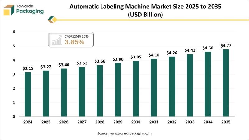
Automatic Labeling Machine Market Set for Strong Growth Through 2035
The global automatic labeling machine market is poised for steady expansion, rising from USD 3.4 billion in 2026 to USD 4.77 billion by 2035 at a CAGR of 3.85%. Demand is being driven by rapid automation in packaging lines, stringent labeling regulations, and the shift toward high-speed, error-free production across industries.
Download Sample: https://www.towardspackaging.com/download-sample/5882
Self-adhesive labeling systems currently hold the largest share at 39%, supported by their versatility and cost efficiency. Meanwhile,…

Unleashing Growth in the Liquid Packaging Market with Strategic Innovations
The liquid packaging industry is experiencing remarkable growth, with projections indicating an increase from USD 397.36 billion in 2025 to USD 645.43 billion by 2034. This growth, at a compound annual growth rate (CAGR) of 5.7%, signifies the expanding demand for liquid packaging solutions across a variety of sectors. As we delve into the market dynamics, it becomes clear that the liquid packaging sector is evolving rapidly, with several key…

Advancements in Hot-Fill Food Packaging Paving the Way for a Sustainable Future
The global hot-fill food packaging market is experiencing a steady rise, with an expected market value of USD 71.26 billion by 2033, up from USD 49.85 billion in 2023. This growth is projected to follow a compound annual growth rate (CAGR) of 3.76% from 2024 to 2033, reflecting the increasing demand for innovative packaging solutions in the food and beverage sector.
Download a Brochure of Hot-fill Food Packaging Market: https://www.towardspackaging.com/download-brochure/5266
Hot-Fill…

Driving Growth and Innovation in the Plastic Bag Market
The plastic bag market is undergoing significant growth, with its value reaching an estimated US$ 25.10 billion in 2023. Projections suggest that this market could hit a substantial US$ 35.41 billion by 2033, marking a steady compound annual growth rate (CAGR) of 3.5% from 2024 to 2034. This growth is largely driven by the expanding needs of various industries for efficient and cost-effective packaging solutions.
Download a Brochure of Plastic Bag…
More Releases for TSV
TSV Electroplating Additive Market Size, Growth Opportunities and Forecast 2025- …
Los Angeles, United State: A newly published report titled "Global TSV Electroplating Additive Market Insights, Forecast to 2025-2031" by QY Research throws light on the industry dynamics and current and future trends that play a key role in determining the business expansion. The global TSV Electroplating Additive market was valued at US$ 224 million in 2024 and is anticipated to reach US$ 372 million by 2031, witnessing a CAGR of…
Through Silicon Via (TSV) Technology Market 2022 | Detailed Report
The Through Silicon Via (TSV) Technology report compiles the market information depending upon market development and growth factors, optimizing the growth path. In addition, it highlights the strategies and market share of the leading vendors in the particular market. The report follows a robust research methodology model that helps to make informed decisions. It obtains both qualitative and quantitative market information supported by primary research.
The Through Silicon Via (TSV) Technology…
Through Silicon Via (TSV) Technology Market 2021 | Detailed Report
Global Through Silicon Via (TSV) Technology Market 2021-2027, has been prepared based on an in-depth market analysis with inputs from industry experts. The report covers the market landscape and its growth prospects in the coming years. The report includes a discussion of the key vendors operating in this market. An exclusive data offered in this report is collected by research and industry experts team.
Get Free Sample PDF (including full TOC,…
3D TSV and 2.5D Market Size, Share, Development by 2024
Market Research Report Store offers a latest published report on 3D TSV and 2.5D Market Analysis and Forecast 2019-2025 delivering key insights and providing a competitive advantage to clients through a detailed report.
The global 3D TSV and 2.5D market is valued at xx million USD in 2018 and is expected to reach xx million USD by the end of 2024, growing at a CAGR of xx% between 2019 and 2024.
The…
Global 3D TSV Market Share and Growth 2019 - QY Research
3D TSV is a vertical electrical connection (via) that passes completely through a silicon wafer or die. TSVs are high performance interconnect techniques used as an alternative to wire-bond and flip chips to create 3D packages and 3D integrated circuits. Compared to alternatives such as package-on-package, the interconnect and device density is substantially higher, and the length of the connections becomes shorter.
The global 3D TSV market is valued at xx…
3D TSV Packages Market Value Chain and Forecast 2016-2026
Currently, 3D Packaging using Through Silicon Via technology (3D TSV) is one of the hottest topics in the semiconductor ecosystem. 3D TSV is vertical electrical connection (via) passing completely through a silicon wafer or die. These short vertical interconnects are replacing the long interconnects of 2D packaging technologies including wire-bond and flip chips.
Growing demand for high density and multifunctional microelectronics with improved performance, and the reduction of timing delays is…
