Press release
A Brief Introduction of Wafer Paddle | Semicera
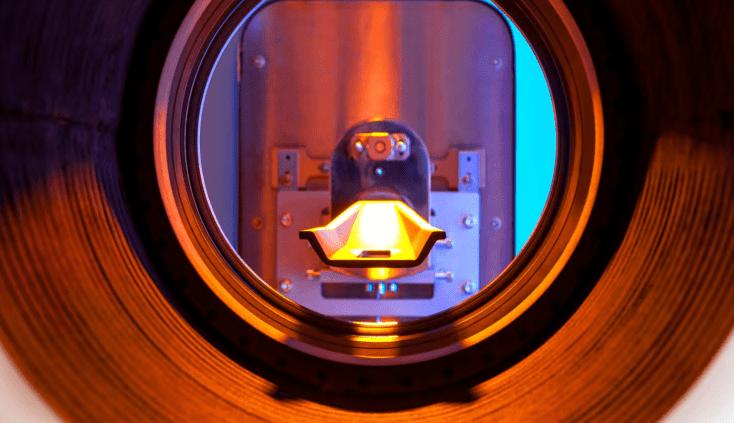
A wafer paddle is a crucial component used in the semiconductor and photovoltaic industries to handle wafers during high-temperature processes. At Semicera, we take pride in our advanced capabilities to produce top-quality wafer paddles that meet the rigorous demands of these sectors. Our wafer paddles ensure safe, precise handling of wafers, contributing to the efficiency and reliability of the entire manufacturing process.
At Semicera, we have developed a specialized range of wafer paddles with various purity levels, tailored to different industry needs. For the photovoltaic industry, we provide wafer paddles made from 2N purity sintered silicon carbide (RBSiC) and 2N recrystallized silicon carbide, ensuring superior performance in high-temperature environments. These materials offer excellent resistance to wear, corrosion, and thermal shock, making them ideal for photovoltaic applications.
In the semiconductor industry, where precision and material purity are paramount, Semicera offers wafer paddles made from 3-4N purity recrystallized silicon carbide (RSiC) and Si-Impregnated Silicon Carbide parts. These wafer paddles are designed to handle the rigorous demands of semiconductor fabrication processes, such as chemical vapor deposition (CVD), etching, and oxidation, ensuring minimal contamination and maximum durability.
For industries requiring even higher purity levels, Semicera offers wafer paddles made from RSiC combined with CVD SiC, achieving purity levels of 5N-6N. These ultra-pure materials are perfect for next-generation semiconductor technologies, where any impurities can compromise the functionality of sensitive electronic components. By offering such high purity, Semicera ensures that our wafer paddles meet the most stringent demands of cutting-edge manufacturing processes.
At Semicera, our manufacturing process combines precision engineering with advanced materials to produce wafer paddles that excel in performance and durability. Our ability to meet the specific needs of both the photovoltaic and semiconductor industries demonstrates our versatility and commitment to quality. Whether it's 2N RBSiC for photovoltaics or 5N-6N RSiC + CVD SiC for semiconductors, Semicera's expertise allows us to deliver wafer paddles that support the most advanced technologies.
Media Contact
Company Name: Semicera
Email:Send Email [https://www.abnewswire.com/email_contact_us.php?pr=a-brief-introduction-of-wafer-paddle-semicera]
Country: China
Website: https://www.semi-cera.com/
This release was published on openPR.
Permanent link to this press release:
Copy
Please set a link in the press area of your homepage to this press release on openPR. openPR disclaims liability for any content contained in this release.
You can edit or delete your press release A Brief Introduction of Wafer Paddle | Semicera here
News-ID: 3661461 • Views: …
More Releases from ABNewswire

Top 5 Tips for Choosing the Best Driving Lights for Any Vehicle
Picking out the right driving lights [https://www.jgledlight.com/driving-lights/] for your vehicle can really make a difference when it comes to safety and visibility on the road. Honestly, with so many options out there, it can get pretty overwhelming. Every type has its own perks, but not all of them are going to be ideal for every car or driving situation.Think about what you actually need and prefer. If you're often out…

An Engineer's Guide to Thread-Forming Screws for Thermoplastics
Selecting the right screw for a thermoplastic assembly requires coordination between thread geometry, resin properties, boss design, and installation settings. PT-style thread-forming screws, often using a narrow flank angle of about 30 degrees, can reduce radial stress and widen the assembly torque window. The final design should still be tested with the actual resin and molded component.
Why Plastic Fastening Requires Special Attention
Thermoplastics are widely used in automotive parts, electronics, medical…
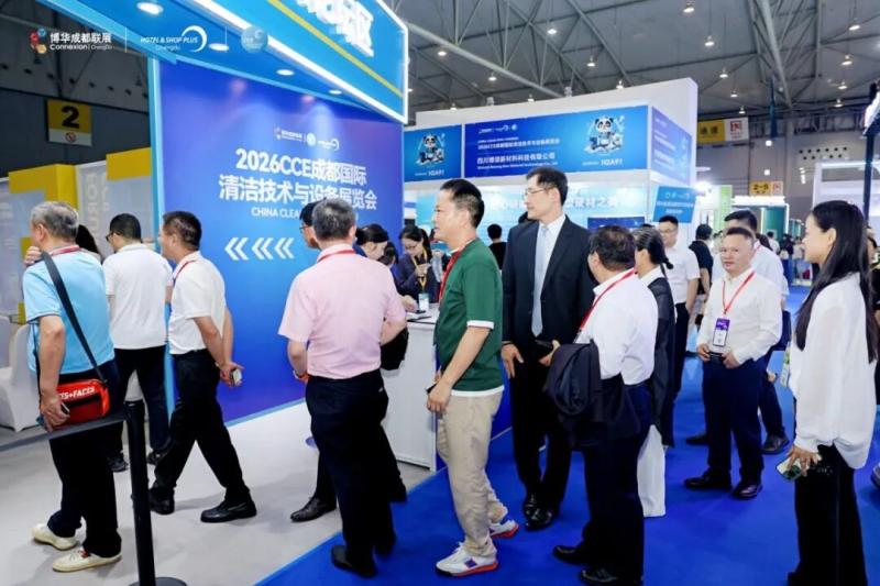
Yiwei Auto Joins 2026 Chengdu CCE Forum to Advance Green Mobility
Image: https://www.1vtrucktech.com/uploads/chengdu-CCE-expo2.jpg
From July 2 to 4, the 2026 Chengdu CCE International Cleaning Expo was successfully held. Leveraging this industry platform, Yiwei Auto actively participated in the Sanitation Industry Supply and Demand Exchange Forum and the Entrepreneurs' Roundtable, while also hosting the "Yiwei Night" Industry Networking Dinner. Bringing together industry associations, technical experts, and partners from across the sanitation value chain, the event fostered collaboration, knowledge sharing, and innovation to explore…
Complete Guide to Electrode Die-Cutting Machine Selection: Scientific Decision-M …
In the vast industrial chain of lithium battery manufacturing, electrode Die-Cutting is a critical process that bridges upstream and downstream operations. Its precision and efficiency directly determine cell performance, safety, and manufacturing costs. In the past, high-end electrode die-cutting technology was long monopolized by European, American, Japanese, and Korean companies, becoming one of the bottlenecks constraining China's new energy industry development. Today, through continuous innovation, domestic manufacturers represented by Dongguan…
More Releases for Semicera
Why is a CVD coating focus ring for etching critical for high-precision semicond …
CVD coating focus rings play a critical role in modern semiconductor etching by stabilizing plasma boundaries and ensuring uniform ion distribution across the wafer. This article explains why they are essential for advanced nodes, highlighting their impact on etch uniformity, CD control, contamination reduction, and overall process yield.
. From Plasma Etching to Focused Ring Engineering
Plasma etching is one of the most critical patterning technologies in modern semiconductor manufacturing, enabling the…
Semiconductor Graphite Fixture: A Critical Process Component in Semiconductor Ma …
In semiconductor manufacturing, numerous key materials and components determine process stability and product yield. While not as widely recognized as wafers or targets, semiconductor graphite fixtures [https://www.vet-china.com/high-purity-graphite-chuck-fixture-for-single-crystal-growth.html/] play an indispensable role in high-temperature processing, epitaxial growth, annealing, and compound semiconductor fabrication.
Simply put, semiconductor graphite fixtures are functional components used in high-temperature process equipment, primarily undertaking tasks like load-bearing, support, positioning, and heat transfer. They are typically made from high-purity graphite…
Gallium Oxide Single Crystal Substrate Market Growth Analysis, Latest Industry T …
QY Research has recently published a research report titled, "Global Gallium Oxide Single Crystal Substrate Market Share and Ranking, Overall Sales and Demand Forecast 2025-2031", assessing various factors impacting its trajectory. The research study offers deep evaluation of the global Gallium Oxide Single Crystal Substrate market and helps market participants to gain a strong foothold in the industry. It sheds light on critical market dynamics such as drivers, restraints, trends,…
Global and U.S. Quartz Focus Rings Market Report, Published by QY Research.
Quartz Focus Rings are precision-engineered consumable components used in semiconductor etching systems, designed to stabilize plasma uniformity and protect wafers during etch processes. Manufactured from high-purity fused silica, these rings exhibit superior thermal resistance, low contamination, and excellent dielectric properties, making them essential for advanced logic and memory chip fabrication.
https://www.qyresearch.com/reports/4916820/quartz-focus-rings
The global Quartz Focus Rings market reached USD 367 million in 2024, expanding at a CAGR of 6.2% through 2030, driven…
What is Porous Graphite? Features and Applications
Porous graphite revolutionizes SiC crystal growth [https://www.semi-cera.com/tac-coating-monocrystal-growth-parts/] by improving yield, reducing defects, and lowering production costs.
Introduction:
Porous graphite [https://www.semi-cera.com/porous-graphite-tube-product/], also known as porous carbon or porous graphite materials, is a specially designed form of graphite featuring interconnected pore networks. This unique material offers superior performance in a range of applications, particularly in the silicon carbide (SiC) crystal growth process. By playing a pivotal role in balancing gas-phase components, isolating trace impurities,…
A Brief Introduction of SiC Paddle | Semicera
Image: https://m191.goodao.net/uploads/SiC-Paddle.png
A SiC paddle is a vital component used in high-tech manufacturing processes, particularly in the semiconductor and photovoltaic industries. Made from silicon carbide (SiC), these paddles are designed to transport and handle wafers during high-temperature processes like etching, deposition, and oxidation. As a leading manufacturer of advanced ceramic solutions, Semicera produces top-quality SiC paddles that meet the stringent demands of modern manufacturing, ensuring precision, durability, and excellent thermal performance.
For…
