Press release
Value of E-Beam Wafer Inspection System Market Estimated at US$ 6.1 Billion by 2031, TMR Study

E-Beam Wafer Inspection System
E-Beam Wafer Inspection System market is estimated to attain a valuation of US$ 6.1 Bn by the end of 2031, states a study by Transparency Market Research (TMR). Besides, the report notes that the market is prognosticated to expand at a CAGR of 20.3% during the forecast period, 2023-2031
𝐃𝐨𝐰𝐧𝐥𝐨𝐚𝐝 𝐒𝐚𝐦𝐩𝐥𝐞 𝐎𝐟 𝐭𝐡𝐞 𝐑𝐞𝐩𝐨𝐫𝐭 -https://www.transparencymarketresearch.com/sample/sample.php?flag=S&rep_id=15884
Advanced semiconductor devices often have complex structures and multiple layers. E-beam wafer inspection systems can analyze these structures at high resolution, enabling the detection of defects that may impact device performance or reliability. Thus, shrinking semiconductor devices and their complex structure are driving the e-beam wafer inspection system industry growth.
One of the notable e-beam wafer inspection system market trends is the development and adoption of multi e-beam wafer inspection systems. This trend is driven by the need for higher throughput, improved defect detection, and enhanced process control in semiconductor manufacturing. These systems offer promising capabilities to meet the evolving challenges of semiconductor technology nodes and advanced packaging techniques. Companies compete in the market by continually improving their e-beam wafer inspection systems, enhancing defect detection capabilities, increasing throughput, and offering advanced analytics and data management features.
𝐈𝐧𝐪𝐮𝐢𝐫𝐞 𝐛𝐞𝐟𝐨𝐫𝐞 𝐩𝐮𝐫𝐜𝐡𝐚𝐬𝐞 - https://www.transparencymarketresearch.com/sample/sample.php?flag=EB&rep_id=15884
𝐒𝐡𝐫𝐢𝐧𝐤𝐢𝐧𝐠 𝐒𝐞𝐦𝐢𝐜𝐨𝐧𝐝𝐮𝐜𝐭𝐨𝐫 𝐃𝐞𝐯𝐢𝐜𝐞 𝐍𝐨𝐝𝐞𝐬 𝐭𝐨 𝐃𝐫𝐢𝐯𝐞 𝐄-𝐁𝐞𝐚𝐦 𝐖𝐚𝐟𝐞𝐫 𝐈𝐧𝐬𝐩𝐞𝐜𝐭𝐢𝐨𝐧 𝐒𝐲𝐬𝐭𝐞𝐦 𝐌𝐚𝐫𝐤𝐞𝐭 𝐆𝐫𝐨𝐰𝐭𝐡
Advanced device manufacturers are continuously shrinking semiconductor device nodes, and they are now adopting cutting-edge EUV (Extreme Ultraviolet) technology for lithography. EUV technology enables rapid and highly precise lithography processes, contributing to the ongoing reduction in device dimensions.
The adoption of EUV lithography is shrinking the dimensions of circuit pattern dimensions, which in turn is boosting the demand for reliable, accurate, and repeatable inspection and measurement systems in order to manage production lines and optimize yields. This is especially important to ensure the quality of advanced EUV masks and minimizing variations in circuit dimensions, as well as detecting stochastic defects that are characteristic of EUV lithography.
Consequently, demand for high-throughput, high-resolution inspection and measurement solutions is increasing in order to keep up with the growing number of inspection targets in the semiconductor manufacturing process.
𝐂𝐨𝐦𝐩𝐞𝐭𝐢𝐭𝐨𝐫 𝐀𝐧𝐚𝐥𝐲𝐬𝐢𝐬:
Applied Materials Inc., ASML Holding N.V., Hitachi Ltd., HOLON CO., LTD., KLA Corporation, MKS Instruments, Inc., PDF Solutions, Photo electron Soul Inc., TASMIT, Inc., Telemark Factory, ZEISS Semiconductor Manufacturing Technology.
𝐌𝐚𝐫𝐤𝐞𝐭 𝐒𝐞𝐠𝐦𝐞𝐧𝐭𝐚𝐭𝐢𝐨𝐧 -
𝐓𝐲𝐩𝐞
Single Beam
Multi Beam
Wafer Node
Mature Nodes (Above 10nm)
Advance Nodes (10nm, 7nm, 5nm, below)
𝐀𝐩𝐩𝐥𝐢𝐜𝐚𝐭𝐢𝐨𝐧
Logic Chips
Memory Chips
Others
𝐄𝐧𝐝-𝐮𝐬𝐞 𝐈𝐧𝐝𝐮𝐬𝐭𝐫𝐲
Automotive
Consumer Electronics
IT & Telecom
Industrial
Others (Aerospace and Defense, Healthcare, etc.)
𝐇𝐚𝐯𝐞 𝐀𝐧𝐲 𝐐𝐮𝐞𝐫𝐲? 𝐀𝐬𝐤 𝐓𝐨 𝐀𝐧𝐚𝐥𝐲𝐬𝐭: https://www.transparencymarketresearch.com/sample/sample.php?flag=ASK&rep_id=15884
𝐊𝐞𝐲 𝐃𝐞𝐯𝐞𝐥𝐨𝐩𝐦𝐞𝐧𝐭𝐬
In 2021, Hitachi launched an e-beam inspection system for EUV 3nm and 5nm processes. The GS1000 is a high-end standard electron beam inspection system. It is a combination of a high-performance electron optical system and a high-speed, large-capacity data processing system that offers solutions to issues that arise when implementing EUV lithography into semiconductor device mass-production.
On July 20, 2020, KLA Corporation launched the breakthrough eSL10TM e-beam patterned-wafer defect inspection technology. The novel technology is expected to reduce delivery time for high-performance logic and memory chips, especially those that rely on extreme ultraviolet (EUV) lithography, by detecting and reporting faults that cannot be routinely caught by optical or other e-beam defect detection platforms.
𝐓𝐡𝐢𝐬 𝐑𝐞𝐩𝐨𝐫𝐭 𝐥𝐞𝐭𝐬 𝐲𝐨𝐮 𝐢𝐝𝐞𝐧𝐭𝐢𝐟𝐲 𝐭𝐡𝐞 𝐨𝐩𝐩𝐨𝐫𝐭𝐮𝐧𝐢𝐭𝐢𝐞𝐬 𝐢𝐧 𝐄-𝐁𝐞𝐚𝐦 𝐖𝐚𝐟𝐞𝐫 𝐈𝐧𝐬𝐩𝐞𝐜𝐭𝐢𝐨𝐧 𝐒𝐲𝐬𝐭𝐞𝐦 𝐌𝐚𝐫𝐤𝐞𝐭 𝐛𝐲 𝐦𝐞𝐚𝐧𝐬 𝐨𝐟 𝐚 𝐫𝐞𝐠𝐢𝐨𝐧:
North America (the United States, Canada, and Mexico)
Europe (Germany, UK, France, Italy, Russia, Turkey, etc.)
Asia-Pacific (China, Japan, Korea, India, Australia, and Southeast Asia (Indonesia, Thailand, Philippines, Malaysia, and Vietnam))
South America (Brazil etc.) The Middle East and Africa (North Africa and GCC Countries)
𝐌𝐨𝐫𝐞 𝐓𝐫𝐞𝐧𝐝𝐢𝐧𝐠 𝐑𝐞𝐩𝐨𝐫𝐭𝐬 𝐛𝐲 𝐓𝐫𝐚𝐧𝐬𝐩𝐚𝐫𝐞𝐧𝐜𝐲 𝐌𝐚𝐫𝐤𝐞𝐭 𝐑𝐞𝐬𝐞𝐚𝐫𝐜𝐡 -
𝐋𝐚𝐛𝐨𝐫𝐚𝐭𝐨𝐫𝐲 𝐆𝐚𝐬 𝐆𝐞𝐧𝐞𝐫𝐚𝐭𝐨𝐫𝐬 𝐌𝐚𝐫𝐤𝐞𝐭- https://www.globenewswire.com/news-release/2022/08/18/2500847/0/en/Laboratory-Gas-Generators-Market-to-Expand-at-CAGR-of-11-during-Forecast-Period-notes-TMR-Study.html
𝐇𝐨𝐬𝐩𝐢𝐭𝐚𝐥 𝐀𝐜𝐪𝐮𝐢𝐫𝐞𝐝 𝐃𝐢𝐬𝐞𝐚𝐬𝐞 𝐓𝐞𝐬𝐭𝐢𝐧𝐠 𝐌𝐚𝐫𝐤𝐞𝐭- https://www.globenewswire.com/news-release/2022/08/18/2501052/0/en/Hospital-Acquired-Disease-Testing-Market-to-Reach-US-2-85-Bn-by-2027-observes-TMR-Study.html
𝐀𝐛𝐨𝐮𝐭 𝐔𝐬 𝐓𝐫𝐚𝐧𝐬𝐩𝐚𝐫𝐞𝐧𝐜𝐲 𝐌𝐚𝐫𝐤𝐞𝐭 𝐑𝐞𝐬𝐞𝐚𝐫𝐜𝐡
Transparency Market Research, a global market research company registered at Wilmington, Delaware, United States, provides custom research and consulting services. The firm scrutinizes factors shaping the dynamics of demand in various markets. The insights and perspectives on the markets evaluate opportunities in various segments. The opportunities in the segments based on source, application, demographics, sales channel, and end-use are analysed, which will determine growth in the markets over the next decade.
Our exclusive blend of quantitative forecasting and trends analysis provides forward-looking insights for thousands of decision-makers, made possible by experienced teams of Analysts, Researchers, and Consultants. The proprietary data sources and various tools & techniques we use always reflect the latest trends and information. With a broad research and analysis capability, Transparency Market Research employs rigorous primary and secondary research techniques in all of its business reports.
𝐂𝐨𝐧𝐭𝐚𝐜𝐭 𝐔𝐬
Nikhil Sawlani
Transparency Market Research Inc.
CORPORATE HEADQUARTER DOWNTOWN,
1000 N. West Street,
Suite 1200, Wilmington, Delaware 19801 USA
Tel: +1-518-618-1030
USA - Canada Toll Free: 866-552-3453
This release was published on openPR.
Permanent link to this press release:
Copy
Please set a link in the press area of your homepage to this press release on openPR. openPR disclaims liability for any content contained in this release.
You can edit or delete your press release Value of E-Beam Wafer Inspection System Market Estimated at US$ 6.1 Billion by 2031, TMR Study here
News-ID: 3340916 • Views: …
More Releases from Transparency Market Research
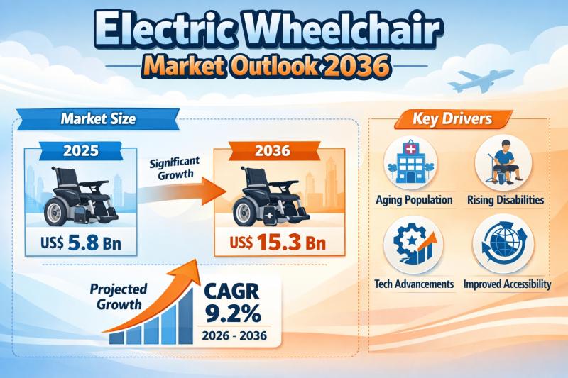
Electric Wheelchair Market Expanding at 9.2% CAGR Through 2036 - By Control Type …
The global electric wheelchair market continues to demonstrate strong and sustained growth, fueled by demographic transitions, technological innovation, and expanding healthcare access worldwide. Valued at US$ 5.8 billion in 2025, the market is projected to reach US$ 15.3 billion by 2036, expanding at a compound annual growth rate (CAGR) of 9.2% from 2026 to 2036.
Discover essential conclusions and data from our Report in this sample -
https://www.transparencymarketresearch.com/sample/sample.php?flag=S&rep_id=4198
This robust trajectory reflects rising…
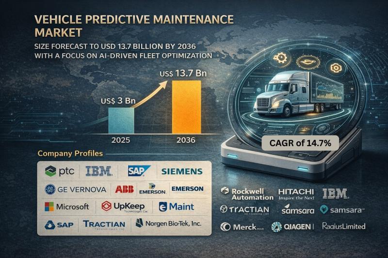
Vehicle Predictive Maintenance Market Size Forecast to USD 13.7 Billion by 2036 …
Vehicle Predictive Maintenance Market Outlook 2036
The global vehicle predictive maintenance market was valued at USD 3 Billion in 2025 and is projected to reach USD 13.7 Billion by 2036, expanding at a robust CAGR of 14.7% from 2026 to 2036. Market growth is driven by increasing adoption of connected vehicles, rising fleet digitalization, advancements in AI-driven analytics, and growing emphasis on minimizing vehicle downtime and maintenance costs.
👉 Get your sample…
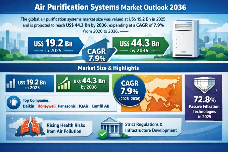
Global Air Purification Systems Market to Reach USD 44.3 Billion by 2036 at 7.9% …
The global Air Purification Systems Market was valued at US$ 19.2 Bn in 2025 and is projected to expand to US$ 44.3 Bn by 2036, registering a compound annual growth rate (CAGR) of 7.9% from 2026 to 2036. The market's upward trajectory reflects the structural shift in indoor air quality (IAQ) management, moving from discretionary consumer spending to mission-critical infrastructure investment.
With historical data available from 2021 to 2024, the industry…
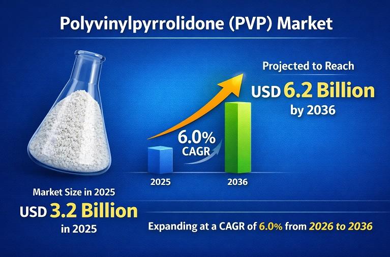
Polyvinylpyrrolidone (PVP) Market to Reach USD 6.2 Billion by 2036 Driven by Pha …
The Polyvinylpyrrolidone (PVP) Market was valued at around US$ 3.2 billion in 2025 and is projected to reach approximately US$ 6.2 billion by 2036, expanding at a steady CAGR of about 6.0% during the forecast period. This growth is primarily driven by rising demand from the pharmaceutical industry, where PVP is widely used as a tablet binder, solubilizer, and stabilizer, along with increasing consumption in cosmetics and personal care products…
More Releases for EUV
EUV Pellicle Market Size, Trends & Forecasts | Valuates Reports
EUV Pellicle Market Size
The global market for EUV Pellicle was valued at US$ 78.8 million in the year 2024 and is projected to reach a revised size of US$ 171 million by 2031, growing at a CAGR of 8.6% during the forecast period.
Get Free Sample: https://reports.valuates.com/request/sample/QYRE-Auto-17Z11340/Global_EUV_Pellicle_Market_Research_Report_2022?utm_source=prnewswire&utm_medium=referral
In a typical semiconductor process, a thin protective film is usually placed on the surface of the photomask to protect it from contaminants. This thin…
Extreme Ultraviolet (EUV) Lithography Market
Extreme Ultraviolet (EUV) Lithography Market Overview
Extreme ultraviolet lithography is an advanced version of lithography which uses an extreme ultra violet light of the shortest wavelength of 13.5 nm. Lithography is mainly used to print complicated patterns which are mostly highlight integrated circuits onto semiconductor wafers.
This report provides a deep insight into the global Extreme Ultraviolet (EUV) Lithography market covering all its essential aspects. This ranges from a macro overview of…
EUV Photoresists Market Revenue, Insights, Overview, Outlook, Analysis
EUV Photoresists Market Size
The global EUV Photoresists market is projected to grow from US$ 226.4 million in 2024 to US$ 878.9 million by 2030, at a Compound Annual Growth Rate (CAGR) of 25.4% during the forecast period.
Get Free Sample: https://reports.valuates.com/request/sample/QYRE-Auto-36H8625/Global_EUV_Photoresists_Market_Insights_Forecast_to_2028
Global key players of EUV Photoresists include TOK, JSR and Shin-Etsu Chemical, etc. The top three players hold a share over 90%. Japan is the largest market, has a share about…
Global EUV Resist Market Research Report 2023-2029
EUV Resist is a material that undergoes a change in its physical properties upon exposure to radiation.EUV lithography uses higher energy radiation to enable smaller feature sizes, and new resist solutions, optimized for use with EUV light exposure, are urgently required.
Global EUV Resist Market: Driven factors and Restrictions factors
The research report encompasses a comprehensive analysis of the factors that affect the growth of the market. It includes an evaluation of…
EUV Lithography Market 2023 Size, Share, Growth Report 2030
Latest Updated Report 2023, The Global EUV Lithography Market to Growing A CAGR of % during forecast period of 2023-2030. The Market is segmented by Global EUV Lithography Market Breakdown by Application (Integrated Device Manufacturers (IDM), Foundry, Others) by Type (Light Source, Exposure Device, EUV Pod, Others) and by Geography (North America, South America, Europe, Asia Pacific, MEA).
The EUV Lithography Market 2023 Report makes available the current and forthcoming technical…
Greatest Progress in EUV Lithography (EUVL) Market, 2021-2026
(Portland, United States): Big Market Research newly added a research report on the EUV Lithography (EUVL) Market which represents a study for the period from 2021 to 2026. The research study provides a near look at the market scenario and dynamics impacting its growth. This report highlights the crucial developments along with other events happening in the market which are marking on the growth and opening doors for future growth…
