Press release
Jenoptik Reports Growing Demand for Gallium Phosphide Microoptics
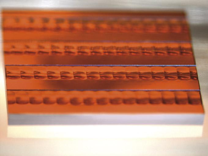
At SPIE BiOS 2013, Jenoptik is presenting high-index gallium phosphide microoptics for near to mid-wavelength infrared applications.Microlenses, microlens arrays, and diffractive optics are used in medical applications for homogenization of laser beams for laser eye surgery and aesthetic skin treatment, for creating multi-spot arrays for ophthalmic diagnostics, for collimating and shaping laser beams for surgical applications, and for imaging applications such as optical coherence tomography and scanning confocal microscopy.
Recent advances in near infrared (NIR) and mid-wavelength infrared (MWIR) quantum cascade
and fiber lasers in conjunction with new diagnostic and treatment approaches are placing new demands on microoptics for these applications. These needs include a broad NIR - MWIR transmission, high numerical aperture (NA), and small form factor for minimally invasive applications. With 15 years of experience, Jenoptik´s Grayscale lithographically fabricated gallium phosphide (GaP) microlenses and microlens arrays meet these demands with:
1) A unique and broad wavelength range from 600 nanometers to beyond 5 mikrometers
2) A high refractive index of 3.1 allowing a single element lens or lens array with NA’s
up to 0.85
3) Complex surface shapes providing for beam collimation and circularization of high divergence diode lasers with a single element
Scanning confocal microscopy and minimally invasive optical coherence tomography are two examples where a single GaP microlens or microlens array can be used to extend the wavelength range over traditional GRIN and Si lenses. Jenoptik’s ability to fabricate complex aspheric elements with high numerical aperture also provide for better imaging performance when compared with GRIN lens based systems.
In addition, standard manufacturing processes are available for a range of different optical materials such as SiO2, GaAs, CaF2, Al2O3, ZnS, ZnSe, Ge, and chalcogenide glass.
Visit us at SPIE BiOS 2013, from February 2nd to 3rd, in San Francisco at the Moscone Center, south hall in booth # 8628.
About the Jenoptik Optical Systems division
Through its Optical Systems division, the Jenoptik Group delivers world-class precision optics and systems designed and manufactured to the highest quality standards.
Besides offering customized systems, modules and assemblies, the Optical Systems division is a development and production partner for optical, microoptical and coated optical components - made of optical glasses, IR materials as well as polymers.
It possesses outstanding expertise in the development and manufacture of optics and microoptics for beam shaping used in the semiconductor industry and laser material processing.
The product portfolio also includes optical and opto-electronic systems and components for applications in defense & security, health care & life science, digital imaging, machine vision as well as lighting.
Uwe Wielsch
Head of Sales Microoptics
JENOPTIK Optical Systems GmbH
Goeschwitzer Strasse 25
07745 Jena I Germany
Phone +49 3641 65-2440 I Fax -443
microoptics.os@jenoptik.com
www.jenoptik.com/microoptics
This release was published on openPR.
Permanent link to this press release:
Copy
Please set a link in the press area of your homepage to this press release on openPR. openPR disclaims liability for any content contained in this release.
You can edit or delete your press release Jenoptik Reports Growing Demand for Gallium Phosphide Microoptics here
News-ID: 250792 • Views: …
More Releases from JENOPTIK Optical Systems GmbH

Optical Systems Division of Jenoptik with new Technologies and Products at Photo …
In San Francisco Jenoptik will be showcasing, from February 4–6, new technologies and further developments of its products from the Optical Systems divisions at Photonics West. Jenoptik is supporting again Entrepreneurs in Photonics in the SPIE Startup Challenge as the Founding Sponsor.
Silverline F-Theta Lenses with Broadband Anti-Reflection Coating for High-Power NIR-Diode-Laser-Applications
Jenoptik has added to its successful Silverline F-Theta product line new broadband F-Theta lenses with less absorption for high power…

Jenoptik introduces new products at Photonics West 2013
On February 5-7, 2013, Jenoptik will be presenting new products and advanced technologies in the fields of optics, lasers and infrared technology in San Francisco. Furthermore, the Group is the main sponsor of the SPIE Startup Challenge 2013 to support young entrepreneurs.
As one of the world’s leading manufacturers of optical systems, Jenoptik will also showcase new ultra-precision optics processed using Ion Beam Figuring (IBF) at Photonics West. The new…
More Releases for Microlens
Global and U.S. Spherical Ball Microlens Market Report, Published by QY Research …
QY Research has released a comprehensive new market report on Spherical Ball Microlenses, miniature optical components designed to focus, collimate, or couple light in extremely compact optical systems. Owing to their spherical geometry, high numerical aperture, and ease of alignment, ball microlenses are widely used in fiber-optic communications, laser coupling, imaging modules, optical sensors, and biomedical devices. As demand accelerates for miniaturized, high-precision optical assemblies in telecommunications, consumer electronics, and…
Global and U.S. Freeform Microlens Arrays Market Report, Published by QY Researc …
A compact 3D-sensing module supplier in South Korea struggled to achieve uniform depth accuracy in its next-generation Time-of-Flight (ToF) cameras used for smartphone facial recognition and robotics. Conventional spherical microlens arrays produced non-uniform illumination patterns, causing dead zones and edge distortion in the projected infrared dot map. This degraded depth reconstruction and increased calibration time during mass production. To solve the issue, the engineering team adopted Freeform Microlens Arrays, which…
Diffractive Microlens Arrays Market Size, Trends, Growth: Global Forecast 2025-2 …
The global market for Diffractive Microlens Arrays was estimated to be worth US$ 873 million in 2024 and is forecast to a readjusted size of US$ 1472 million by 2031 with a CAGR of 7.8% during the forecast period 2025-2031.
Global Leading Market Research Publisher QYResearch announces the release of its latest report "Diffractive Microlens Arrays - Global Market Share and Ranking, Overall Sales and Demand Forecast 2025-2031". Based on current…
Microlens Arrays Market Size, Share, Trends, Market Growth, and Business Strateg …
Microlens Arrays Market Overview -
Microlens arrays are compact optical components consisting of a grid of tiny lenses, each with diameters typically ranging from a few microns to millimeters. These arrays are designed to manipulate light efficiently, offering high precision in applications such as beam shaping, focusing, and light distribution. Their ability to enhance optical performance has made them indispensable in various industries, including imaging, telecommunications, semiconductor industry, and photonics. In…
Microlens Film Market 2024 - By Key Players, Challenges, Regional Overview, Oppo …
The microlens film market has emerged as a significant segment within the optical and display industries, driven by advancements in technology and increasing demand for high-performance optical devices. Microlens films, composed of arrays of tiny lenses that enhance the optical properties of various surfaces, are widely used in applications ranging from displays and lighting to sensors and cameras.
The Microlens Film Market size was estimated at USD 0.57 billion in 2023.…
Microlens Film Market: Growing Need for Enhanced Light Control and Image Quality …
Global Microlens Film Market Overview:
The Microlens Film market is a broad category that includes a wide range of products and services related to various industries. This market comprises companies that operate in areas such as consumer goods, technology, healthcare, and finance, among others.
In recent years, the Microlens Film market has experienced significant growth, driven by factors such as increasing consumer demand, technological advancements, and globalization. This growth has created both…
