Press release
Thin Film Semiconductor Deposition Market 2020 Global Insights and Business Scenario – Applied Materials, Tokyo Electron Limited, Lam Research, Shin-Etsu Chemical and Other.
Thin Film Semiconductor Deposition Market
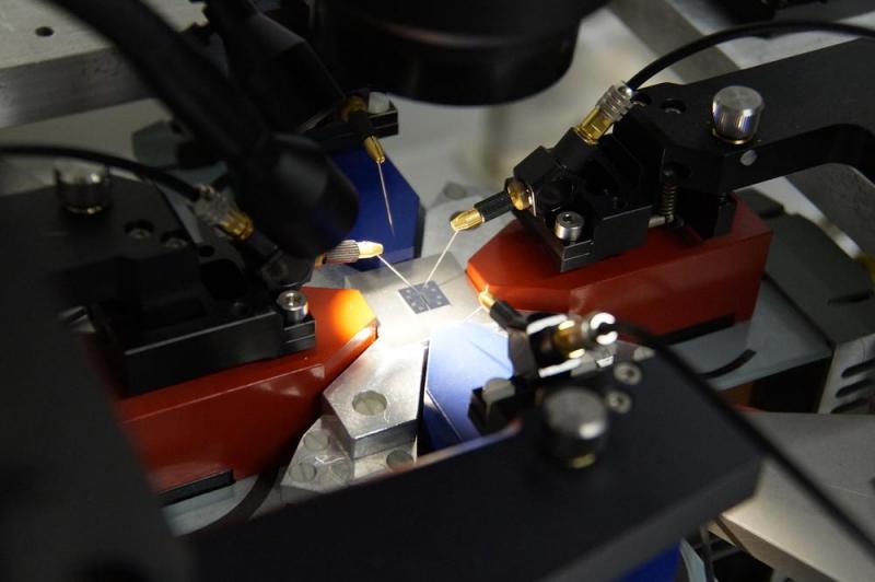
Thin films have a great impact on the modern era of technology. Thin films are considered as backbone for advanced applications in the various fields such as optical devices, environmental applications, telecommunications devices, energy storage devices, and so on . The crucial issue for all applications of thin films depends on their morphology and the stability. The morphology of the thin films strongly hinges on deposition techniques. Thin films can be deposited by the physical and chemical routes. In this chapter, we discuss some advance techniques and principles of thin-film depositions. The vacuum thermal evaporation technique, electron beam evaporation, pulsed-layer deposition, direct current/radio frequency magnetron sputtering, and chemical route deposition systems will be discussed in detail.
Click the link to get a Sample Copy of the Report:
https://www.marketinsightsreports.com/reports/08052201392/global-thin-film-semiconductor-deposition-market-size-status-and-forecast-2020-2026/inquiry?source=Openpr&Mode=12
COMPANIES COVERED (SALES, PRICE, REVENUE, VOLUME, GROSS MARGIN AND MARKET SHARE)- Applied Materials, Tokyo Electron Limited, Lam Research, Shin-Etsu Chemical and Other.
Thin film deposition is the process of creating and depositing thin film coatings onto a substrate material. These coatings can be made of many different materials, from metals to oxides to compounds. Thin film coatings also have many different characteristics which are leveraged to alter or improve some element of the substrate performance. For example, some are transparent; some are very durable and scratch-resistant; and some increase or decrease the conductivity of electricity or transmission of signals.
Thin film deposition is an important manufacturing step in the production of many opto-electronic, solid state and medical devices and products, including consumer electronics, semiconductor lasers, fiber lasers, LED displays, optical filters, compound semiconductors, precision optics, microscopy & microanalysis sample slides, and medical implants. There are a few different technologies and methods that can be used to apply thin film coatings, and an array of tools and equipment that can be used to streamline or enhance the thin film deposition process.
Tokyo Electron to Release EXIM™ Sputtering System for Next-Generation Semiconductor Devices
TOKYO -- Tokyo Electron Limited (TEL) announced today the addition of the EXIMTM sputtering system to the company's product portfolio.
EXIM is a PVD (physical vapor deposition) system developed to form thin-film materials required for advanced semiconductor devices. It is based on ultra-high-vacuum sputtering technology and incorporates newly-developed film deposition techniques to form complex stacks of precision electronic materials. This flexible system can accommodate a variety of process modules to meet specific application needs, and the system can scale flexibly to suit various purposes, ranging from development to volume production.
Early evaluators of EXIM have explored its unique capabilities to form multi-layer magnetic tunnel junction (MTJ) stacks for spin-transfer-torque magnetoresistive random access memories (STT-MRAM). When used to form MTJ stacks with 20 or more layers, EXIM delivered a throughput on the order of 25 wafers per hour. Stacks have been demonstrated with good magnetic memory characteristics, and a TMR (Tunneling magnetoresistance) ratio over 230% with TEL's unique perpendicular MTJ stack
Applied Materials showcases ‘new memory’ PVD equipment
2019.07.19 -- Applied Materials, the world’s largest semiconductor equipment maker unveiled Physical Vapor Deposition (PVD) equipment specialized for new memory production. The company said it is confident of selling $100 million worth this year, Applied Materials Korea said on July 17.
“The combined sales target for the two equipment is $100 million,” said Park Rae-hak, senior vice president of Applied Materials Korea. “We believe they can be applied to mass production lines.”
PVD is a critical part of the chip making process, and it involves metal going from a condensed phase to a vapor phase, and then back to a thin film condensed phase. Until now, the industry had faced hurdles in creating this material for next generation memory chips, such as MRAM, ReRAM and PRAM. On this day, Applied Materials Korea showcased the Endura Clover MRAM PVD and the Endura Impulse PVD. The company said once these equipment make it into the market, it would become much easier to mass produce new chips.
Buy This Report:
https://www.marketinsightsreports.com/report/purchase/08052201392?mode=su?source=Openpr&Mode=12
Market Segmentation:
Segmentation by Type
Chemical Vapor Deposition (CVD)
Physical Vapor Deposition (PVD)
Others (Epitaxy, And Electro Hydrodynamic Deposition)
Segmentation by Application
IT & Telecom
Electronics
Energy & Power
Automotive
Aerospace & Defense
Others (Healthcare and Industrial)
INFLUENCE OF THE THIN FILM SEMICONDUCTOR DEPOSITION MARKET REPORT:
-Comprehensive assessment of all opportunities and risk in the Thin Film Semiconductor Deposition market.
- Thin Film Semiconductor Deposition market recent innovations and major events.
-A detailed study of business strategies for growth of the Thin Film Semiconductor Deposition market-leading players.
-Conclusive study about the growth plot of Thin Film Semiconductor Deposition market for forthcoming years.
-In-depth understanding of Thin Film Semiconductor Deposition market-particular drivers, constraints and major micro markets.
-Favourable impression inside vital technological and market latest trends striking the Thin Film Semiconductor Deposition market.
WHAT ARE THE MARKET FACTORS THAT ARE EXPLAINED IN THE REPORT?
Key Strategic Developments: The study also includes the key strategic developments of the market, comprising R&D, new product launch, M&A, agreements, collaborations, partnerships, joint ventures, and regional growth of the leading competitors operating in the market on regional scale.
Analytical Tools: The Thin Film Semiconductor Deposition Market Report includes the accurately studied and assessed data of the key industry players and their scope in the market by means of a number of analytical tools. The analytical tools such as Porter’s five forces analysis, SWOT analysis, feasibility study, and investment return analysis have been used to analyze the growth of the key players operating in the market.
Key Market Features: The report evaluated key market features, including revenue, price, capacity, capacity utilization rate, gross, production, production rate, consumption, import/export, supply/demand, cost, market share, CAGR, and gross margin. In addition, the study offers a comprehensive study of the key market dynamics and their latest trends, along with pertinent market segments and sub-segments.
The report has 150 tables and figures browse the report description and TOC:
https://www.marketinsightsreports.com/reports/08052201392/global-thin-film-semiconductor-deposition-market-size-status-and-forecast-2020-2026?source=Openpr&Mode=12
FIND OUT:
• Thin Film Semiconductor Deposition market: Where are the opportunities? What does the future look like for Thin Film Semiconductor Deposition? What will be the market size in the next 5 years?
• Market trends: What is driving the market? Where are the key players? What are their strategies? What is holding the market behind? Where is the industry heading for in the short and long-term? How are new developments expected to change the market?
• Technology: How are new technologies shaping the market?
What are the new revenue channels which companies can explore for growth?
Related Reports:
Atomic Layer Deposition (ALD) Equipment Market:
https://www.marketinsightsreports.com/reports/01122521534/global-atomic-layer-deposition-ald-equipment-market-growth-2020-2025?source=Openpr&Mode=12
Semiconductor Deposition Material Market:
https://www.marketinsightsreports.com/reports/01122520649/global-semiconductor-deposition-material-market-growth-2020-2025?source=Openpr&Mode=12
Electron Beam Physical Vapor Deposition (EBPVD) Coating Market:
https://www.marketinsightsreports.com/reports/01122531990/global-electron-beam-physical-vapor-deposition-ebpvd-coating-market-research-report-with-opportunities-and-strategies-to-boost-growth-covid-19-impact-and-recovery?source=Openpr&Mode=12
If you have any questions about any of our “Thin Film Semiconductor Deposition market report” or would like to schedule a personalized free demo of Thin Film Semiconductor Deposition market report, please do not hesitate to contact me at irfan@marketinsightsreports.com.
Best wishes,
Irfan Tamboli
Head of Sales Operations
Market Insights Reports
Tel: + 1704 266 3234 | +91-750-707-8687
Email: sales@marketinsightsreports.com | irfan@marketinsightsreports.com
About Us:
MarketInsightsReports provides syndicated market research on industry verticals including Healthcare, Information and Communication Technology (ICT), Technology and Media, Chemicals, Materials, Energy, Heavy Industry, etc. MarketInsightsReports provides Global and regional market intelligence coverage, a 360-degree market view which includes statistical forecasts, competitive landscape, detailed segmentation, key trends, and strategic recommendations.
This release was published on openPR.
Permanent link to this press release:
Copy
Please set a link in the press area of your homepage to this press release on openPR. openPR disclaims liability for any content contained in this release.
You can edit or delete your press release Thin Film Semiconductor Deposition Market 2020 Global Insights and Business Scenario – Applied Materials, Tokyo Electron Limited, Lam Research, Shin-Etsu Chemical and Other. here
News-ID: 2226283 • Views: …
More Releases from Market Insights Reports

Cold Chain Monitoring Market May See a Big Move | BlueAir, Denso, Eureka Forbes, …
Market Insights Reports published a new research publication on "Cold Chain Monitoring Market Insights, to 2032" with 232 pages and enriched with self-explained Tables and charts in presentable format. In the Study you will find new evolving Trends, Drivers, Restraints, Opportunities generated by targeting market associated stakeholders. The growth of the Cold Chain Monitoring market was mainly driven by the increasing R&D spending across the world.
Some of the key players…

Outbound Logistics Market Next Big Thing | Major Giants- Draexlmaier, Faurecia, …
Market Insights Reports published a new research publication on "Outbound Logistics Market Insights, to 2032" with 232 pages and enriched with self-explained Tables and charts in presentable format. In the Study you will find new evolving Trends, Drivers, Restraints, Opportunities generated by targeting market associated stakeholders. The growth of the Outbound Logistics market was mainly driven by the increasing R&D spending across the world.
Some of the key players profiled in…

Veterinary Telemedicine Market May See a Big Move | Nestle, Deuerer, The J.M. Sm …
Market Insights Reports published a new research publication on "Veterinary Telemedicine Market Insights, to 2032" with 232 pages and enriched with self-explained Tables and charts in presentable format. In the Study you will find new evolving Trends, Drivers, Restraints, Opportunities generated by targeting market associated stakeholders. The growth of the Veterinary Telemedicine market was mainly driven by the increasing R&D spending across the world.
Some of the key players profiled in…

Precision Planting Market is Set to Fly High in Years to Come
Market Insights Reports published a new research publication on "Precision Planting Market Insights, to 2032" with 232 pages and enriched with self-explained Tables and charts in presentable format. In the Study you will find new evolving Trends, Drivers, Restraints, Opportunities generated by targeting market associated stakeholders. The growth of the Precision Planting market was mainly driven by the increasing R&D spending across the world.
Some of the key players profiled in…
More Releases for Deposition
Major Growth Driver Identified in 2025 Chemical Vapor Deposition Market: Rising …
Stay ahead with our updated market reports featuring the latest on tariffs, trade flows, and supply chain transformations.
Chemical Vapor Deposition Market Size Valuation Forecast: What Will the Market Be Worth by 2025?
The market size of chemical vapor deposition has experienced swift expansion in the past few years. Experts predict that it will surge from $38.84 billion in 2024 to a staggering $42.89 billion in 2025, with a compound annual growth…
Atomic Layer Deposition Market: Atomic Layer Deposition Market to Hit USD 6.06B …
Atomic Layer Deposition Market Scope:
Key Insights : Atomic Layer Deposition Market size was valued at USD 2.10 billion in 2022 and is poised to grow from USD 2.36 billion in 2023 to USD 6.06 billion by 2031, growing at a CAGR of 12.50% during the forecast period (2024-2031).
Discover Your Competitive Edge with a Free Sample Report :https://www.skyquestt.com/sample-request/atomic-layer-deposition-market
Access the full 2024 Market report for a comprehensive understanding @https://www.skyquestt.com/report/atomic-layer-deposition-market
In-Depth Exploration of…
Atomic Layer Deposition Market Report 2024 - Atomic Layer Deposition Market Size …
"The Business Research Company recently released a comprehensive report on the Global Atomic Layer Deposition Market Size and Trends Analysis with Forecast 2024-2033. This latest market research report offers a wealth of valuable insights and data, including global market size, regional shares, and competitor market share. Additionally, it covers current trends, future opportunities, and essential data for success in the industry.
According to The Business Research Company's, The atomic layer deposition…
Optical Coating Market, By Technology (Vacuum Deposition Technology, Ion-Assiste …
Market Definition
An optical coating contains one or more thin layers of material deposited on an optical component such as a lens or mirror, which modifies how the optic transmits and reflects light. One type of optical coating is an anti-reflective coating that reduces unwanted reflections from surfaces, and generally used on camera lenses and spectacle. Another type is the high-reflector coating, which can produce mirrors that reflect the light greater than 99.99% of the light and fall on them. More complex…
Vapour Deposition Market Global Industry Analysis By Technology Are Chemical Vap …
Vapour deposition market is going to have a rocket boom for their sales, import, export and revenue in the forecast period of 2018-2025.
The report is generated based on the market type, size of the organization, availability on-premises and the end-users’ organization type, and the availability in areas such as North America, South America, Europe, Asia-Pacific and Middle East & Africa.
The base year for calculation in the report is taken as…
Physical Vapor Deposition Market Global Briefing 2017
Global Physical Vapor Deposition Market Research Report 2017 provides a unique tool for evaluating the market, highlighting opportunities, and supporting strategic and tactical decision-making. This report recognizes that in this rapidly-evolving and competitive environment, up-to-date marketing information is essential to monitor performance and make critical decisions for growth and profitability. It provides information on trends and developments, and focuses on markets and materials, capacities and technologies, and on the changing…
