Press release
Silicon EPI Wafer Market Current and Emerging Trends 2020-2027 | Nichia Corporation, Applied Materials, Sumco Corporation, Epigan, ASM, Global Wafers, Siltronic, Wafer World Inc., Tokyo Electron, and Shin Etsu Chemical Co. Ltd
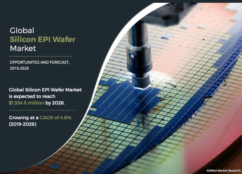
Silicon EPI Wafer Market
The research report provides a detailed study of the recent and emerging market trends, estimations, and qualitative insights on the potential segments of the industry from 2020 to 2027 to understand the fundamental prospects. The report also includes an extensive analysis of the factors that drive and restrain the market growth.
Key Players: Nichia Corporation, Applied Materials, Sumco Corporation, Epigan, ASM, Global Wafers, Siltronic, Wafer World Inc., Tokyo Electron, and Shin Etsu Chemical Co. Ltd.
Download Report Sample (300+ Pages with Latest Industry Insights): https://www.alliedmarketresearch.com/request-sample/6221
Companies nowadays go through market research reports for better understanding of past, present, and future market trends and sales. This aids the market players with proper decision making for further investments. With the help of SWOT analysis, the market report offers an in-depth analysis of driving and restraining factors and upcoming opportunities. Furthermore, report also involves a comprehensive information based on strategic developments, market size, and revenue share estimations of the industry. Moreover, the research report on the Silicon EPI Wafer Market assists to reinforce association along with making useful decision to proliferate the business furthermore.
The information is collected from various primary and secondary sources. The market report also highlights frontrunners in the industry along with analysing their profiles as well as market share. Moreover, the report provides some insights of market strategies followed by these firms such as mergers & acquisition, joint venture, new product launches, expansions, and collaborations. These strategies aid the market players to endure the competition and uphold their strong position in the field.
Key Benefits from Silicon EPI Wafer Market Report 2020-2027:
• The report offers an extensive analysis of the recent Silicon EPI Wafer Market trends, estimations, and market size in between 2020 to 2027 to outline new prospects.
• With Porter's Five Forces analysis, the report highlights the effectiveness of consumers and suppliers to enable the stakeholders with strategic business decisions.
• The report also involves a detailed analysis of key impacting factors & top investment pockets.
• Study based on regional segments along with state wise revenue generation is also included in the report.
Get Detailed COVID-19 Impact Analysis on the Silicon EPI Wafer Market: https://www.alliedmarketresearch.com/request-for-customization/6221?reqfor=covid
Market Segmentation: by Type (Heteroepitaxy and Homoepitaxy), Wafer Size (6-inch, 8-inch, 12-inch, and Others) Application (LED, Power Semiconductor, MEMS- Based Devices), and Industry Vertical (Consumer Electronics, Automotive, Healthcare, Industrial, and Others)
The Silicon EPI Wafer Market report doles out information based on current market developments, trade protocols, import exports, productivity, value chain optimization, and revenue share. In addition, the report also examines the influence of domestic and local market players, upcoming opportunities associated with emerging revenue pockets, strategic analysis on market growth, industry segmentation, geographical expansion, and technological innovations.
The market report offers quantitative study and qualitative aspects of the global market from 2020 to 2027 that assists the stakeholders to gain a proper understanding of the actual market insights. The report consists regional as well as the global market study with key market players and growth schemes. The information provided based on Silicon EPI Wafer Market domain are gathered from highly reliable sources and are precisely examined and affirmed by the research experts. Furthermore the report also highlights the stimulus of the clients and the suppliers to facilitate investors for making appropriate decisions and reinforce their network.
The market is studied across regions including North America, LAMEA, Asia-Pacific, and Europe. The Silicon EPI Wafer Market is thoroughly analysed on the basis of region wise competitive scenarios. These insights assist to make new strategies and gain new opportunities for greater achievements. The report also covers key determinants of the market that plays a significant role in boosting as well as restraining the market growth. This analysis offers an absolute scenario of future enforcement of the market.
For Purchase Inquiry: https://www.alliedmarketresearch.com/purchase-enquiry/6221
At Allied Market Research we purpose to highlight the most beneficial opportunities for our clients. We make sure to offer valuable guidance to make it easier for our clients to work on future strategies along with being prepared for upcoming changes in technology as well as the Silicon EPI Wafer Market trends. Our advisory services aims to support our clients to discover the hidden opportunities and comprehend the challenges as well as competitions.
All together, the report portrays an in-depth synopsis of the Silicon EPI Wafer Market that would assist the industry professionals, equipment manufacturers, existing players, and start-ups to have an idea of present market insights for further strategies to support market centric plans, policies, and investments in the future.
Highlights of the Report:
1. Thorough and comprehensive assessment of the Silicon EPI Wafer Market.
2. Revenues generated by each segment of the market during the forecast period.
3. Key determinants in the market.
4. Strategies followed by the key market players.
5. Opportunities based on regional analysis of market for the key players in the industry.
6. Recent scope and trends in the Silicon EPI Wafer Market.
Buy Now: https://www.alliedmarketresearch.com/checkout-final/4451fad5bbc39c56df46a2950d9fd220
CHAPTER 10: COMPANY PROFILES
10.1. APPLIED MATERIALS. INC.
10.1.1. Company overview
10.1.2. Company snapshot
10.1.3. Operating business segments
10.1.4. Product portfolio
10.1.5. Source: Corporate Publica R&D Expenditure
10.1.6. Business performance
10.1.7. Key strategic moves and developments
10.2. ASM INTERNATIONAL N.V.
10.2.1. Company overview
10.2.2. Company snapshot
10.2.1. Operating business segments
10.2.2. Product portfolio
10.2.3. R&D Expenditure
10.2.4. Business performance
10.2.5. Key strategic moves and developments
10.3. SHOWA DENKO K.K
10.3.1. Company overview
10.3.2. Company snapshot
10.3.3. Operating business segments
10.3.4. Product portfolio
10.3.5. R&D Expenditure
10.3.6. Business performance
10.3.7. Key strategic moves and developments
10.4. GLOBAL WAFER
10.4.1. Company overview
10.4.2. Company snapshot
10.4.3. Product portfolio
10.5. NICHIA CORPORATION
10.5.1. Company overview
10.5.2. Company snapshot
10.5.3. Product portfolio
10.6. SHIN-ETSU CHEMICAL CO., LTD
10.6.1. Company overview
10.6.2. Company snapshot
10.6.3. Operating business segments
10.6.4. Product portfolio
10.6.5. R&D Expenditure
10.6.6. Business performance
10.6.7. Key strategic moves and developments
10.7. SUMCO CORPORATION
10.7.1. Company overview
10.7.2. Company snapshot
10.7.3. Operating business segments
10.7.4. Product portfolio
10.7.5. R&D Expenditure
10.7.6. Business performance
10.8. SILTRONIC
10.8.1. Company overview
10.8.2. Company snapshot
10.8.3. Product portfolio
10.8.4. R&D Expenditure
10.8.5. Business performance
10.9. TOKYO ELECTRON LTD.
10.9.1. Company overview
10.9.2. Company snapshot
10.9.3. Operating business segments
10.9.4. Product portfolio
10.9.5. R&D Expenditure
10.9.6. Business performance
10.10. WAFER WORLD INC.
10.10.1. Company overview
10.10.2. Company snapshot
10.10.3. Product portfolio
10.10.4. Key strategic moves and developments
Read More at https://www.globenewswire.com/news-release/2020/06/08/2044968/0/en/Global-Silicon-EPI-Wafer-Market-to-Reach-1-55-Billion-by-2026-at-4-8-CAGR.html
Contact:
David Correa
5933 NE Win Sivers Drive
#205, Portland, OR 97220
United States
USA/Canada (Toll Free):
+1-800-792-5285, +1-503-894-6022, +1-503-446-1141
UK: +44-845-528-1300
Hong Kong: +852-301-84916
India (Pune): +91-20-66346060
Fax: +1(855)550-5975
help@alliedmarketresearch.com
Web: https://www.alliedmarketresearch.com
About Us
Allied Market Research (AMR) is a full-service market research and business-consulting wing of Allied Analytics LLP based in Portland, Oregon. Allied Market Research provides global enterprises as well as medium and small businesses with unmatched quality of "Market Research Reports" and "Business Intelligence Solutions." AMR has a targeted view to provide business insights and consulting to assist its clients to make strategic business decisions and achieve sustainable growth in their respective market domain.
We are in professional corporate relations with various companies and this helps us in digging out market data that helps us generate accurate research data tables and confirms utmost accuracy in our market forecasting. Every data presented in the reports published by us is extracted through primary interviews with top officials from leading companies of domain concerned. Our secondary data procurement methodology includes deep online and offline research and discussion with knowledgeable professionals and analysts in the industry.
This release was published on openPR.
Permanent link to this press release:
Copy
Please set a link in the press area of your homepage to this press release on openPR. openPR disclaims liability for any content contained in this release.
You can edit or delete your press release Silicon EPI Wafer Market Current and Emerging Trends 2020-2027 | Nichia Corporation, Applied Materials, Sumco Corporation, Epigan, ASM, Global Wafers, Siltronic, Wafer World Inc., Tokyo Electron, and Shin Etsu Chemical Co. Ltd here
News-ID: 2195676 • Views: …
More Releases from Allied Market Research
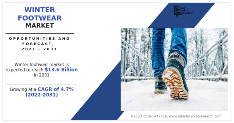
Winter Footwear Market 2026 : Expeditious Growth Expected in 2021 - 2031 | UGG, …
According to a new report published by Allied Market Research, titled, "Winter Footwear Market," The winter footwear market was valued at $8.6 billion in 2021, and is estimated to reach $13.6 billion by 2031, growing at a CAGR of 4.7% from 2022 to 2031.
"Numerous varieties of winter footwear are expected to boost the market growth in the foreseeable future. Moreover, incorporation of customization, as well as innovative winter footwear is…

Ergonomic Chair Market Research Insights: Uncovering CAGR and USD Growth Drivers …
An ergonomic office chair is mostly utilized in different firms and other business areas where employees operate in a sitting position for extended hours. Adjustable seats, brackets and natural postures, which minimize back discomfort and stress in the lengthy seating time, are the ergonomic chairs. Currently, the offices are selecting ergonomic office chairs over the standard office chair to make the workplace healthier, happier, and to boost employer productivity. The…
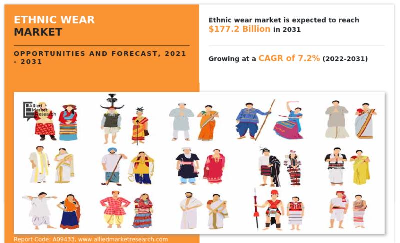
Ethnic Wear Market Forecasting Essentials: Interpreting CAGR and USD Projections …
According to a new report published by Allied Market Research, titled, "Ethnic Wear Market," The ethnic wear market size was valued at $89.3 billion in 2021, and is estimated to reach $177.2 billion by 2031, growing at a CAGR of 7.2% from 2022 to 2031.
The market for ethnic wear is mostly driven by the rising number of fashion influencers across the globe. It is difficult to overlook the importance of…
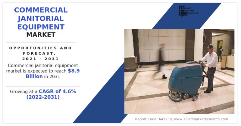
$8.9+ Billion Commercial Janitorial Equipment Market Value by 2031 with a 4.6% C …
According to a new report published by Allied Market Research, titled, "Commercial Janitorial Equipment Market," The commercial janitorial equipment market size was valued at $5.7 billion in 2021, and is estimated to reach $8.9 billion by 2031, growing at a CAGR of 4.6% from 2022 to 2031. There has been a surge in the number of restaurants, hotels, and hospitals across the globe, which further contribute to the demand for…
More Releases for Wafer
Semiconductor Silicon Wafer Market Is Going to Boom |• Silicon Wafer • Globa …
Worldwide Market Reports has released a new in-depth research study on the "Semiconductor Silicon Wafer Market," highlighting strong growth potential in the coming years. The report delivers a structured and data-driven analysis of the market landscape, combining robust research methodology, market sizing, validated data modeling, and insights sourced from reliable primary and secondary channels.
The study thoroughly examines key market aspects, including growth drivers, restraints, challenges, emerging opportunities, technological advancements, innovation…
Semiconductor Wafer Electrostatic Chucks for 300mm Wafer Market Size, Trends & F …
Semiconductor Wafer Electrostatic Chucks for 300mm Wafer Market Size
The global Semiconductor Wafer Electrostatic Chucks for 300mm Wafer market is projected to grow from US$ 1227 million in 2024 to US$ 1672.7 million by 2030, at a Compound Annual Growth Rate (CAGR) of 5.3% during the forecast period.
Get Free Sample: https://reports.valuates.com/request/sample/QYRE-Auto-38F13137/Global_Semiconductor_Wafer_Electrostatic_Chucks_for_300mm_Wafer_Market_Research_Report_2023?utm_source=openpr&utm_medium=referral
The US & Canada market for Semiconductor Wafer Electrostatic Chucks for 300mm Wafer is estimated to increase from $ million in…
Wafer Hybrid Bonding Equipment Market Share Driven by Wafer-to-Wafer Technology …
Wafer Hybrid Bonding Equipment Market Size
The global market for Wafer Hybrid Bonding Equipment was valued at US$ 164 million in the year 2024 and is projected to reach a revised size of US$ 756 million by 2031, growing at a CAGR of 24.7% during the forecast period.
View sample report
https://reports.valuates.com/request/sample/QYRE-Auto-31W14822/Global_Wafer_Hybrid_Bonding_Equipment_Market_Insights_Forecast_to_2029
The Wafer Hybrid Bonding Equipment market is experiencing accelerated growth, driven by increasing demand for advanced semiconductor packaging technologies that enable higher…
Semiconductor Wafer Electrostatic Chucks for 300mm Wafer Market
Semiconductor Wafer Electrostatic Chucks for 300mm Wafer Market
The global Semiconductor Wafer Electrostatic Chucks for 300mm Wafer market was valued at US$ 1165 million in 2023 and is anticipated to reach US$ 1672.7 million by 2030, witnessing a CAGR of 5.3% during the forecast period 2024-2030.
View Sample Report
https://reports.valuates.com/request/sample/QYRE-Auto-38F13137/Global_Semiconductor_Wafer_Electrostatic_Chucks_for_300mm_Wafer_Market_Research_Report_2023
Report Scope
The Semiconductor Wafer Electrostatic Chucks for 300mm Wafer market size, estimations, and forecasts are provided in terms of output/shipments (Units) and revenue…
Automatic Mounter Wafer Equipment Market Report 2018: Segmentation by Type (100 …
Global Automatic Mounter Wafer Equipment market research report provides company profile for Lintec Corporation, Nitto Denko, Tokyo Electron, Technovision, Takatori, Ultron Systems, DISCO Corp., Syagrus Systems, Advanced Dicing Technologies, Longhill Industries and Others.
This market study includes data about consumer perspective, comprehensive analysis, statistics, market share, company performances (Stocks), historical analysis 2012 to 2017, market forecast 2018 to 2025 in terms of volume, revenue, YOY growth rate, and CAGR for…
EMEA Solar Wafer Cutting Fluid PEG Market For Semiconductor, Solar Wafer, Crysta …
Latest industry research report on: EMEA (Europe, Middle East and Africa) Solar Wafer Cutting Fluid PEG Market : Industry Size, Share, Research, Reviews, Analysis, Strategies, Demand, Growth, Segmentation, Parameters, Forecasts
Request For Sample Report @ https://www.marketresearchreports.biz/sample/sample/1194694
Geographically, this report split EMEA into Europe, the Middle East and Africa, With sales (K MT), revenue (Million USD), market share and growth rate of Solar Wafer Cutting Fluid PEG for these regions, from 2012 to…
