Press release
Plan Optik joins C2MI Network

After successfully working with C2MI and members of their company network in the past years Plan Optik AG will from now on also participate in C2MI network activities. Joining this network will enable Plan Optik to share their experience and Know-how to members, partners and companies beyond. As a member Plan Optik will provide manufacturing service for other members, partners and other companies in order to thrive innovations and decrease the time from prototype to product manufacturing of new technologies.
About C2MI:
„The C2MI is an international beacon in advanced packaging and microsystems. As a Centre of Excellence, its goal is to allow its members to foster the growth of the microelectronics industry through the accelerated commercialization of market-driven prototypes. Active and seamless collaboration and synergy among the Center’s members enables the rapid commercialization of next-generation prototypes.“ (from C2MI Homepage)
www.c2mi.ca
www.planoptik.com
About Plan Optik
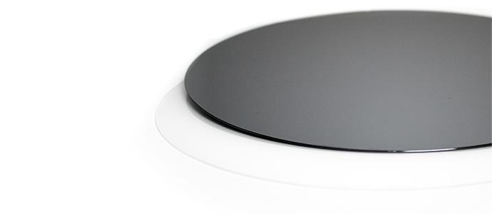
Plan Optik AG is the leading manufacturer of structured wafers when it comes to technology. In sectors such as consumer electronics, automotive, aerospace, chemistry and pharmaceuticals these wafers are essential components used as active elements for numerous applications in MEMS technology. The wafers of glass, glass-silicon compounds or quartz are available in sizes up to 300 mm diameter.
Wafers by Plan Optik provide high-precision surface roughness in the ångström range (= ten millionths of a millimeter), which are achieved through the use of the MDF polishing process developed by the company. Plan Optik wafers are available to minimum tolerances with application-specific structuring and complex material combinations.
With its subsidiary companies Little Things Factory and MMT, Plan Optik also covers the microfluidics sector, where it is one of the few companies offering complete systems. This is a field in which increasing application possibilities are being developed, for example in medicine and chemistry. It thus offers a growth potential which is approximately as high as the previous core business, wafer technology. For more information, please visit our homepage: www.planoptik.com
Plan Optik AG
Über der Bitz 3
56479 Elsoff · Germany
T +49 2664 5068 0
F +49 2664 5068 91
info@planoptik.com
www.planoptik.com
Press contact:
Markus Wagner
Marketing
T +49 2664 5068 28
m.wagner@planoptik.com
This release was published on openPR.
Permanent link to this press release:
Copy
Please set a link in the press area of your homepage to this press release on openPR. openPR disclaims liability for any content contained in this release.
You can edit or delete your press release Plan Optik joins C2MI Network here
News-ID: 1527473 • Views: …
More Releases from Plan Optik AG
Carriers for mechanical release
Plan Optik AG offers re-usable carriers for thin wafer handling which can be used for mechanical release of the device wafers.
There is an ongoing wafer thickness reduction in the semiconductor industry since years. The market is demanding for smaller devices, cost reduction and increased number of functions. Therefore smaller package sizes need to be generated. Mainly consumer applications are driving this progression but the demand for smaller package sizes is…
