Press release
Global Thin Wafer Market Projected to Augment at a Notable CAGR during the Forecast Period until 2025
Thin Wafer Market
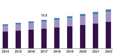
The Thin Wafer market was valued at Million US$ in 2017 and is projected to reach Million US$ by 2025, at a CAGR of during the forecast period. In this study, 2017 has been considered as the base year and 2018 to 2025 as the forecast period to estimate the market size for Thin Wafer.
This report presents the worldwide Thin Wafer market size (value, production and consumption), splits the breakdown (data status 2013-2018 and forecast to 2025), by manufacturers, region, type and application. This study also analyzes the market status, market share, growth rate, future trends, market drivers, opportunities and challenges, risks and entry barriers, sales channels, distributors and Porter's Five Forces Analysis.
Request for PDF Sample of this Report@ http://supplydemandmarketresearch.com/home/contact/79369?ref=Sample-and-Brochure&toccode=SDMREN79369
The following manufacturers are covered in this report:
• LG Siltronic
• Shin-Etsu Chemical
• Siltronic AG
• SUMCO Corporation
• SunEdision Semiconductor
• SUSS MicroTec AG
• Lintec Corporation
• DISCO Corporation
• 3M
• Applied Materials
• Nissan Chemical Corporation
• Synova
• EV Group
• Brewer Science
• Ulvac
Thin Wafer Breakdown Data by Type
• 125mm
• 200mm
• 300mm
Thin Wafer Breakdown Data by Application
• MEMS
• CMOS Image Sensors
• Memory
• RF Devices
• LEDs
• Interposers
• Logic
Request for Discount on this report@ http://supplydemandmarketresearch.com/home/contact/79369?ref=Discount&toccode=SDMREN79369
Thin Wafer Production Breakdown Data by Region
• United States
• Europe
• China
• Japan
• Other Regions
The study objectives of this report are:
• To analyze and research the global Thin Wafer status and future forecast,involving, production, revenue, consumption, historical and forecast.
• To present the key Thin Wafer manufacturers, production, revenue, market share, and recent development.
• To split the breakdown data by regions, type, manufacturers and applications.
• To analyze the global and key regions market potential and advantage, opportunity and challenge, restraints and risks.
• To identify significant trends, drivers, influence factors in global and regions.
• To analyze competitive developments such as expansions, agreements, new product launches, and acquisitions in the market.
Access full research report@ http://supplydemandmarketresearch.com/home/toc_publisher/79369?code=SDMREN79369
Contact Us
info@supplydemandmarketresearch.com
http://supplydemandmarketresearch.com
Phone Number: +919607371825
About Supply Demand Market Research(SDMR)
We have a strong network of high powered and experienced global consultants who have about 10+ years of experience in the specific industry to deliver quality research and analysis.
Having such an experienced network, our services not only cater to the client who wants the basic reference of market numbers and related high growth areas in the demand side, but also we provide detailed and granular information using which the client can definitely plan the strategies with respect to both supply and demand side.
302-20 Misssisauga Valley, Missisauga,
L5A 3S1
This release was published on openPR.
Permanent link to this press release:
Copy
Please set a link in the press area of your homepage to this press release on openPR. openPR disclaims liability for any content contained in this release.
You can edit or delete your press release Global Thin Wafer Market Projected to Augment at a Notable CAGR during the Forecast Period until 2025 here
News-ID: 1451387 • Views: …
More Releases from Supply Demand Market Research

Germany Waste Heat Recovery Systems is anticipated to reach USD 2150 Million by …
The Germany Waste Heat Recovery Systems (WHRS) is anticipated to reach USD 2150 million by 2030 growing at a CAGR of 5.7% from 2024-2030. Continued expansion post-2026 aligns with Germany's decarbonization trajectory, as operators increasingly prioritize heat-recovery to reduce fuel consumption and comply with tightening carbon-intensity expectations.
By technology, the exchange waste heat recovery boilers market size is anticipated to reach USD 710 million by 2030. Exchange/WH Boilers and SRC (Steam…

South Korea Flounder Market Anticipated to grow at a CAGR of 8% from 2023-2030
The South Korea flounder is anticipated to grow at a CAGR% of 8.0% from 2022-2030. The factors contributing towards the high growth are flounders such as halibut and turbot high-protein and low-calorie food, helps to re-solve the nutritional imbalance from diet because of its rich minerals, carbohydrates and vitamins despite low-calorie. They also offer medical benefits as liver of halibut contains lots of vitamin B1 and B2, which is effective…

Global Flounder Market Anticipated to reach USD 56 Billion by 2030
The global flounder market is anticipated to reach USD 56 Billion by 2030, growing at a CAGR% of 8.0% from 2022-2030. The factors contributing towards the high growth are flounders such as halibut and turbot high-protein and low-calorie food, helps to re-solve the nutritional imbalance from diet because of its rich minerals, carbohydrates and vitamins despite low-calorie. They also offer medical benefits as liver of halibut contains lots of vitamin…

Global Seafood Market Anticipated to reach USD 730 Billion by 2030
The global seafood market is anticipated to reach USD 730 Billion by 2030, growing at a CAGR% of 8.9% from 2022-2030. The factors contributing towards the high growth are increased disposable income, awareness of fish being used as an ingredient in healthy food is growing. USA the government plans to sanction illegal fishing activities, actively promote fair trade, and promote strategies to promote the fishing industry through detailed strategies such…
More Releases for Wafer
Semiconductor Silicon Wafer Market Is Going to Boom |• Silicon Wafer • Globa …
Worldwide Market Reports has released a new in-depth research study on the "Semiconductor Silicon Wafer Market," highlighting strong growth potential in the coming years. The report delivers a structured and data-driven analysis of the market landscape, combining robust research methodology, market sizing, validated data modeling, and insights sourced from reliable primary and secondary channels.
The study thoroughly examines key market aspects, including growth drivers, restraints, challenges, emerging opportunities, technological advancements, innovation…
Semiconductor Wafer Electrostatic Chucks for 300mm Wafer Market Size, Trends & F …
Semiconductor Wafer Electrostatic Chucks for 300mm Wafer Market Size
The global Semiconductor Wafer Electrostatic Chucks for 300mm Wafer market is projected to grow from US$ 1227 million in 2024 to US$ 1672.7 million by 2030, at a Compound Annual Growth Rate (CAGR) of 5.3% during the forecast period.
Get Free Sample: https://reports.valuates.com/request/sample/QYRE-Auto-38F13137/Global_Semiconductor_Wafer_Electrostatic_Chucks_for_300mm_Wafer_Market_Research_Report_2023?utm_source=openpr&utm_medium=referral
The US & Canada market for Semiconductor Wafer Electrostatic Chucks for 300mm Wafer is estimated to increase from $ million in…
Wafer Hybrid Bonding Equipment Market Share Driven by Wafer-to-Wafer Technology …
Wafer Hybrid Bonding Equipment Market Size
The global market for Wafer Hybrid Bonding Equipment was valued at US$ 164 million in the year 2024 and is projected to reach a revised size of US$ 756 million by 2031, growing at a CAGR of 24.7% during the forecast period.
View sample report
https://reports.valuates.com/request/sample/QYRE-Auto-31W14822/Global_Wafer_Hybrid_Bonding_Equipment_Market_Insights_Forecast_to_2029
The Wafer Hybrid Bonding Equipment market is experiencing accelerated growth, driven by increasing demand for advanced semiconductor packaging technologies that enable higher…
Semiconductor Wafer Electrostatic Chucks for 300mm Wafer Market
Semiconductor Wafer Electrostatic Chucks for 300mm Wafer Market
The global Semiconductor Wafer Electrostatic Chucks for 300mm Wafer market was valued at US$ 1165 million in 2023 and is anticipated to reach US$ 1672.7 million by 2030, witnessing a CAGR of 5.3% during the forecast period 2024-2030.
View Sample Report
https://reports.valuates.com/request/sample/QYRE-Auto-38F13137/Global_Semiconductor_Wafer_Electrostatic_Chucks_for_300mm_Wafer_Market_Research_Report_2023
Report Scope
The Semiconductor Wafer Electrostatic Chucks for 300mm Wafer market size, estimations, and forecasts are provided in terms of output/shipments (Units) and revenue…
Automatic Mounter Wafer Equipment Market Report 2018: Segmentation by Type (100 …
Global Automatic Mounter Wafer Equipment market research report provides company profile for Lintec Corporation, Nitto Denko, Tokyo Electron, Technovision, Takatori, Ultron Systems, DISCO Corp., Syagrus Systems, Advanced Dicing Technologies, Longhill Industries and Others.
This market study includes data about consumer perspective, comprehensive analysis, statistics, market share, company performances (Stocks), historical analysis 2012 to 2017, market forecast 2018 to 2025 in terms of volume, revenue, YOY growth rate, and CAGR for…
EMEA Solar Wafer Cutting Fluid PEG Market For Semiconductor, Solar Wafer, Crysta …
Latest industry research report on: EMEA (Europe, Middle East and Africa) Solar Wafer Cutting Fluid PEG Market : Industry Size, Share, Research, Reviews, Analysis, Strategies, Demand, Growth, Segmentation, Parameters, Forecasts
Request For Sample Report @ https://www.marketresearchreports.biz/sample/sample/1194694
Geographically, this report split EMEA into Europe, the Middle East and Africa, With sales (K MT), revenue (Million USD), market share and growth rate of Solar Wafer Cutting Fluid PEG for these regions, from 2012 to…
