Press release
Global E-beam Wafer Inspection System Market Advent of Substitute Inspection Systems Hindering Market’s Trajectory

Besides this, experts have observed a considerable rise in the number of mergers and acquisitions conducted over the past few years. Considering the dynamic business environment, companies are encouraged by the cynical nature of the semiconductor industry to enter into strategic collaborations. “Acquiring smaller companies, provides the market players a chance to expand their product portfolio and geographic footprint,” said a lead TMR analyst. The global e-beam wafer inspection system market will therefore witness a considerable rise in the number of mergers and acquisitions in the coming years.
Browse The Press Release: http://www.transparencymarketresearch.com/pressrelease/e-beam-wafer-inspection-system-market.htm
Overall the market will exhibit an impressive 17.5% CAGR between 2017 and 2025. At this pace, the market is projected to reach US$1.06 bn by the end of 2025, from a valuation of US$248.3 million in 2016.
e beam wafer inspection system market
Asia Pacific to Remain Dominant Regional Market
Based on application, the defect imaging segment held dominance in the market with a share of 38.5% in 2016. Through the course of the forecast period, the segment is forecast to remain dominant in the market. Regionally, holding just a little short of 60% of the global e-beam wafer inspection system market, Asia Pacific emerged dominant in 2016. The growing number of electric component manufacturers in the region is expected to help Asia Pacific retain its dominance in the market through the course of the forecast period.
Demand for Miniaturization to Boost Implementation of E-beam Wafer Inspection Systems
Wafers are crucial components integrated within compact devices. For these devices to perform long and error-free, inspecting any defects in them is considered imperative. E-beam wafer inspection system helps in detecting the presence of any faults or defects in MEMs, smartphones, laptops, or other compact devices. Therefore, with the rising demand for miniaturization aimed at improving overall performance across industries, the utility of e-beam wafer inspection systems will grow in response, thus giving impetus to their market.
An e-bean is used to detect defects in voltage-contrast as well as extremely small defects. It thus provides fine resolution at a snap of a finger. E-beam wafer inspection systems also help in minimizing the charging of wafer surface by providing clear and sharper image of defects. This is a crucial factor aiding the market’s expansion worldwide. Furthermore, the demand for high-quality wafers, for use across diverse industries has positively influenced the market. Spurred by these factors, the global e-beam wafer inspection system market is forecast to report strong growth during the forecast period.
Considering the aforementioned factors, the market will significantly gain from the rising operations in the semiconductor industry. Especially in developing regions, where governments are putting in extra effort to bolster industrialization, growth is on cards for the semiconductor industry. This in turn will fuel opportunities for the global e-beam wafer inspection system market.
Advent of Substitute Inspection Systems Hindering Market’s Trajectory
On the downside, the increasing demand for substitute inspection systems will emerge as a major challenge for the market. Technologies such as focused ion beam, terahertz wafer scanner, and optical technology inspection system have made their presence felt in the wafer inspection system market, which does not bring a good news for the e-beam wafer inspection system market. Besides this, the e-beam wafer inspection system market is still reeling under the high cost of implementation, which has a negative impact on its overall prospects.
Nevertheless, growth in multi-beam inspection system holds considerable market opportunities. Its rising use in detecting defects below 2nm, will enable growth of the global e-beam wafer inspection system market in the coming years.
Make an Enquiry @ http://www.transparencymarketresearch.com/sample/sample.php?flag=S&rep_id=15884
This review is based on a TMR report, titled “E-Beam Wafer Inspection System Market (Type - Less Than 1 nm, 1 to 10 nm, and More Than 10 nm; Application - Defect Imaging, Lithographic Qualification, Bare Wafer OQC/IQC, Wafer Dispositioning, Reticle Quality Inspection, and Inspector Recipe Optimization) - Global Industry Analysis, Size, Share, Growth, Trends and Forecast 2017 - 2025.”
Transparency Market Research (TMR) is a market intelligence company, providing global business information reports and services. Our exclusive blend of quantitative forecasting and trends analysis provides forward-looking insight for thousands of decision makers. TMR’s experienced team of analysts, researchers, and consultants, use proprietary data sources and various tools and techniques to gather, and analyze information. Our business offerings represent the latest and the most reliable information indispensable for businesses to sustain a competitive edge
US Office Contact
90 State Street, Suite 700
Albany, NY 12207
Tel: +1-518-618-1030
USA - Canada Toll Free: 866-552-3453
Email: sales@transparencymarketresearch.com
Website: http://www.transparencymarketresearch.com
This release was published on openPR.
Permanent link to this press release:
Copy
Please set a link in the press area of your homepage to this press release on openPR. openPR disclaims liability for any content contained in this release.
You can edit or delete your press release Global E-beam Wafer Inspection System Market Advent of Substitute Inspection Systems Hindering Market’s Trajectory here
News-ID: 594264 • Views: …
More Releases from Transparecny Market Research

HAZMAT Packaging Market Share, Trends, Growth, Forecast By 2027
The global HAZMAT Packaging Market is estimated to flourish at a CAGR of 5.8% from 2024 to 2027.
The overall HAZMAT Packaging industry delivers an in-depth systematic framework and competitive outlook of the HAZMAT Packaging Market from a worldwide perspective. The report starts with a summary of the market, chain structure, and the past as well as current market size. Also, the growth opportunities prevalent in the market in the coming…
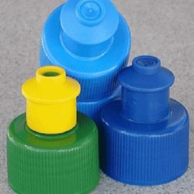
Push Pull Closures Market Will Generate New Growth Opportunities by 2027 with To …
The global Push Pull Closures Market is estimated to flourish at a CAGR of 4.8% from 2024 to 2027.
The overall Push Pull Closures industry delivers an in-depth systematic framework and competitive outlook of the Push Pull Closures Market from a worldwide perspective. The report starts with a summary of the market, chain structure, and the past as well as current market size. Also, the growth opportunities prevalent in the market…
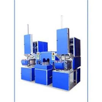
PET Preform Machines Market Estimated to Touch USD 14.1 billion at a CAGR of 6.0 …
The global PET Preform Machines Market has been sailing through robust waters, witnessing a valuation of US$ 8.3 Bn 2022. As we set our sights on the horizon, the market is poised to embark on a journey of steady growth, with a projected Compound Annual Growth Rate (CAGR) of 6.0% from 2023 to 2031. By the end of 2031, the industry is expected to anchor at an impressive US$ 14.1…

Flexible Packaging Paper Market Share, Trends, Growth, Forecast By 2029
The global Flexible Packaging Paper Market has been sailing through robust waters, witnessing a valuation of US$ 47.5 Bn 2021. As we set our sights on the horizon, the market is poised to embark on a journey of steady growth, with a projected Compound Annual Growth Rate (CAGR) of 4.1% from 2023 to 2029. By the end of 2029, the industry is expected to anchor at an impressive US$ 65.2…
More Releases for Wafer
Automatic Mounter Wafer Equipment
Automatic Mounter Wafer Equipment market report offers a detailed assessment of Automatic Mounter Wafer Equipment including upcoming technologies, future prospects, and research methodology. Automatic Mounter Wafer Equipment market report provides market insight by the buyer, suppliers, production, consumption, market size, and growth rate.
Automatic Mounter Wafer Equipment market report covers market drivers, key opportunities, challenges, and threats. Additionally, Automatic Mounter Wafer Equipment market report helps to understand the scenario of the…
Automatic Mounter Wafer Equipment Market Report 2018: Segmentation by Type (100 …
Global Automatic Mounter Wafer Equipment market research report provides company profile for Lintec Corporation, Nitto Denko, Tokyo Electron, Technovision, Takatori, Ultron Systems, DISCO Corp., Syagrus Systems, Advanced Dicing Technologies, Longhill Industries and Others.
This market study includes data about consumer perspective, comprehensive analysis, statistics, market share, company performances (Stocks), historical analysis 2012 to 2017, market forecast 2018 to 2025 in terms of volume, revenue, YOY growth rate, and CAGR for…
Optical Patterned Wafer Inspection Equipment Market: Used for the Detection of D …
Market Outlook
During the process of manufacturing, optical patterned wafer inspection equipments are used for the detection of defects in patterned wafer. As a result of increasing application of semiconductor wafer in various industrial segments such as automotive and consumer electronics among others, the demand for optical patterned wafer inspection equipments is growing. The optical patterned wafer inspection equipments comprises of two technologies, namely; bright-field inspection and dark-field inspection.
The market…
Global Solar Silicon Wafer Market By Product Type | Single Crystal Silicon Wafer …
Researchmoz added Most up-to-date research on "Global Solar Silicon Wafer Market By Product Type | Single Crystal Silicon Wafer and Polycrystalline Silicon Wafer" to its huge collection of research reports.
In this report, the global Solar Silicon Wafer market is valued at USD XX million in 2017 and is expected to reach USD XX million by the end of 2025, growing at a CAGR of XX% between 2017 and 2025.
Geographically, this…
EMEA Solar Wafer Cutting Fluid PEG Market For Semiconductor, Solar Wafer, Crysta …
Latest industry research report on: EMEA (Europe, Middle East and Africa) Solar Wafer Cutting Fluid PEG Market : Industry Size, Share, Research, Reviews, Analysis, Strategies, Demand, Growth, Segmentation, Parameters, Forecasts
Request For Sample Report @ https://www.marketresearchreports.biz/sample/sample/1194694
Geographically, this report split EMEA into Europe, the Middle East and Africa, With sales (K MT), revenue (Million USD), market share and growth rate of Solar Wafer Cutting Fluid PEG for these regions, from 2012 to…
Argon Annealed Wafer Market - Growing Application Of Argon Annealed Wafer In Aut …
The argon annealed wafer is a progressive prime wafer which delivers a defect-free surface region for internal gettering and high device yield for resistance to contamination. Such adaptable features of argon annealed wafer have facilitated the scientists to explore potentials of its application in several fields of consumer application such as wearable and communication devices among others. These highly developed wafers are produced by annealing custom-made substrates. Graphene is being…